By Tahar Allag
The wearable and personal-electronics industries are booming. Devices in this market vary wildly by application and use. These multifunction devices are designed to help people in their daily activities and make their lives comfortable. They can be found in different shapes, colors, sizes, and safety measures. They may differ significantly from each other, but they all have one thing in common—the need for a battery and a battery charger.
These portable devices are typically powered by batteries installed internal to the device, which must be charged efficiently and quickly on a regular basis. The user’s charging experience also needs to meet the requirement of safety, comfort, and convenience.
This article presents the trade-offs between linear chargers and switch-mode chargers. Specific challenges arise with each topology when used to charge a battery pack in wearable applications. The differences between linear and switch-mode topologies are described with details about how each topology can address the requirements of wearable and personal electronic devices. These details range from thermal performance to cost, including size, application area, features and flexibility, electromagnetic interference (EMI), bill-of-material (BOM) counts, charge time, and so on. Finally, there is an evaluation for which charger topology serves which type of requirement best. Understanding charger-related system-level details enables the designer to save both time and cost.
Introduction to battery chargers
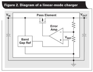
Battery chargers can be generally classified into two topologies: switch and linear-mode. Figures 1 and 2 show the basic architecture of each control topology. As expected, both topologies have pros and cons.
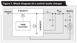
Switch-mode chargers use two power FETs (high-side and low-side) to control the current going into an inductor. Compared to linear chargers, they are more complex and require a larger application area with a higher BOM count. They also require an external inductor and additional capacitors. However, the efficiency of switch-mode chargers will be higher and thermal performance will be better than linear chargers. Switch-mode chargers are also better suited for applications that require higher charge currents. In addition, the switch-mode topology is more flexible and easier to adjust.
Alternatively, the linear charger uses a pass transistor to drop the adapter voltage down to the battery voltage. These are simple chargers that require a small application area and low BOM count, and are limited to a few capacitors and resistors. No inductor is required and no additional capacitors are needed. Efficiency and thermal performance are inferior when compared to switch-mode chargers in high-power applications. These chargers work well for low-power applications where size, BOM, and cost are important.
As shown by Figure 2, a linear charger has the battery pack and the system connected to the device’s same VOUT pin. This non-power-path architecture provides a simpler and lower-cost charger solution, but with some limitations like inadvertent charge termination and system operation with a deeply discharged battery.
Thermal performance
Many wearable devices are required to touch human skin. For example, a smart watch has direct contact with the wearer’s skin while being worn. It would be uncomfortable if the device’s temperature rises above a certain threshold. The thermal budget during use and after charge should be contained. Thus, during device charging, the battery charger’s thermal performance is important and should be as low as possible.
A battery charger’s thermal rise is due to power losses that manifest as thermal rise on the printed circuit board (PCB). The efficiency and power dissipation of a switchmode charger is well contained, whereas a linear charger depends on the voltage drop across the linear regulator times the delivered current.
The power losses of a linear charger reduce significantly as the charger current drops below 300 mA. Figure 3 compares the thermal performance of a linear charger to that of a switch-mode charger with a 300-mA charge current, a battery voltage of 4.0 V, and 5-V input from the adapter. There is only 1ºC difference between the two topologies.
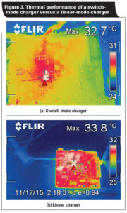
The thermal difference between the two chargers in Figure 3 is negligible; however, as the power increases, a switch-mode charger becomes more suitable. Note that thermal performance of any charger depends on many other factors. For instance, the package type dictates the thermal dissipation of the die, layout of power traces, number of board layers, the amount of copper in a layer, dimension of the board, number and the size of the vias, shape of the board, and so on. For example, the quad-flat no-lead (QFN) package has better thermal performance than the wafer-chip-scale package (WCSP). More layers in the PCB help to dissipate power more easily. Figure 3b, for example, shows that the thermal dissipation is spread evenly over the board. This board layout allows the IC heat to dissipate more easily, thus lowering the device’s peak temperature.
Application area and BOM cost
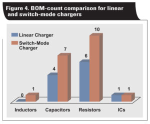
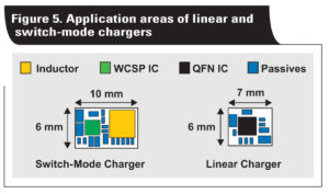
Application area of a charger is important as the total budgeted area for wearable devices is limited. Linear chargers are simple chargers that do not require additional inductor and complex circuitry around the device. Figure 4 compares the BOM count between switch-mode and linear chargers. It shows the minimum number of capacitors, ICs, resistors, and inductors required to design each of these charging topologies. In each of these comparison categories, the linear charger solution has overall fewer components. Nevertheless, switch-mode charger application areas have improved in the last few years and the BOM count has reduced significantly. The inductor is required for switching, but the size of the inductor can shrink with higher-performance devices, which reduces the footprint on the board.
The lower BOM count in a linear charger can translate into application area savings. Any passive elements not used saves space needed for the charger. An inductor is not needed in a linear charger, which also saves space as shown in Figure 5. In low-power applications where space is critical, linear chargers can be a better fit.
Vendors such as Texas Instruments (TI) are pushing the envelope of innovation to meet market demand by reducing the BOM cost and board space without sacrificing device performance. For example, the bq24250 is a highly integrated switch-mode, single-cell Lithium-Ion (Li-Ion) battery charger and system power-path management IC targeted for space-limited, portable applications with highcapacity batteries.
Electromagnetic interference
The simplest component of EMI is an electromagnetic wave that consists of two elements: electric (E-field) and magnetic (H-field) waves running perpendicular to each other. One of the key sources of emissions is a rapid change in a current flow in a loop. A current flowing through a loop can generate a magnetic field, which is proportional to the area of the loop. Loop area is defined as the trace length in a PCB times the distance to the ground plane.
As current changes rapidly in a switch-mode charger, commonly from the internal MOSFETs, an electric field is generated from the voltage transition. Thus, radiation occurs as a result of this current loop. Another source of conducted EMI is ripple in the switching converter’s output. The ripple generally appears at the harmonics of the switching frequency.
EMI can appear as electrical noise on the PCB traces. This high-frequency noise is not limited to just the charge area. Because capacitive and inductive crosstalk occurs between traces that run parallel for even a short distance, noise can propagate all over the PCB traces to cause further disturbances.
Many techniques can be used to reduce EMI in switchmode chargers, such as the addition of shielding, relocating the PCB, changing the switching frequency, and so on. This can add to the cost and increase the application area. For low-noise applications, linear chargers are the safest and easiest solution to reduce EMI.
Design flexibility
Being able to repurpose the same chip for various products or multiple generations has a direct cost savings for expandable system designs. It also shortens the application learning curve and helps to avoid any unnecessary risk by using a known working solution.
The market is pushing for a family of battery chargers that integrate several features to provide flexibility for different applications. The I2C interface can provide that flexibility because it allows each application to be tailored as needed. In I2C mode, designers can program various parameters such as charge current, input current limit, regulation voltage, and termination level. TI has many switch-mode chargers that support I2C bus control of charging parameters.
Switch-mode chargers are known as feature-rich devices. Earlier versions of linear chargers lacked flexibility, while the newer generation of linear chargers offers programmability using external components. The bq24072 and bq24232 linear chargers provide a great deal of design flexibility, including programmable fast charge, pre-charge current, current limit, safety timer, and termination current level. They also come with different regulation voltages and power levels. However, this flexibility adds some cost in the form of increased complexity, application area, and BOM count.
Charge time
The charge cycle of Li-Ion batteries is mainly composed of three phases: pre-charger (trickle), fast charge (constant current), and taper (constant voltage). The transition between one phase to another is not ideal for many chargers. Both voltage and current do not have a sharp transition. TI is the first manufacturer to develop chargetime optimization of the charge cycle for switch-mode chargers to improve this transition. This technique reduces charge time for a given charge rate compared to other solutions.
Also, switch-mode chargers can handle higher voltages from adapters and charge at higher rates without affecting thermal performance. Linear chargers are typically limited to applications with a low input voltage. With these two features, switch-mode chargers can deliver faster charge times compared to the linear topology.
Conclusion
Both linear and switch-mode chargers are attractive when using them to charge low-power applications. Linear chargers are simple and cost-effective to design and no inductor or switching circuitry is required, thus no EMI issues. On the other hand, switch-mode chargers are more efficient, and thermally perform better. They provide more features and improved flexibility. Their charge time is improved with a wider range of input voltages. In conclusion, it is up to the system designer to weigh the pros and cons of each topology with the requirements of the desired end product.
References
- Jinrong Qian and Yevgen Barsukov, “Battery Power Management for portable devices,” ISBN-10: 1608074919; ISBN-13: 978-1608074914, Artech House, May 1, 2013
- Battery Management Solutions for Wearable and Fitness Devices, Texas Instruments selection guide (SLPT034C), 2014
- Tahar Allag, “Selecting the Best bq2407x, bq2423x Single Cell Battery Charger for your Application,” Texas Instruments Application Note (SLUA659), November 2012
- Tahar Allag, “Selecting the Best bq2404x, bq2405x, or bq2409x Single Cell Battery Charger for Your Application,” Texas Instruments Application Note (SLUA667), December 2012
Tahar Allag is a Systems Engineer, Switching Charger Solutions, Battery Charging Products at Texas Instruments, Inc.
