by Ken Ghadia, Production Manager, TechnoTronix
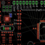
PCB manufacturing process is quite expensive and needs a diligent design tool to be used. There are several PCB designs tools available in the industry for free download.
It’s always suggested to use the latest tools available in the market, and the free tool should be simple to use – practical considerations like the tool’s operating platform (Windows, Linux, Mac) and if it is browser-based need to be evaluated.
Here we are discussing four such free PCB design tools that can build a high-quality circuit board.
KiCad EDA
KiCad is one of the best-rated open-source Electronic Design Automation (EDA) tools available in the market.
Key features:
- KiCad software suite includes a bunch of tools: KiCad – Project manager, Eeschema – Schematic editor, Pcbnew – layout editor, and GerbView – Gerber viewer
- Additional three utility tools: Bitmap2Component – Component maker for logos, PcbCalculator – to calculate components for regulation, transmission lines, etc., Pl Editor – Page layout editor.
- The tool runs on Windows, Linux, and macOS.
- No board-size limitations (can handle up to 32 copper layers)
- Provides all necessary files for PCB manufacturing (Gerber files, drilling files, component location files)
- Offers a SPICE-based simulation engine that supports analog, digital and mixed-signal circuit simulations.
Advantages of KiCad tool:
- Simple User Interface (UI), easy installation, and set-up processes make it an excellent choice for any novice user.
- Advanced features like simulations support, 3D viewer (generates a quick 3D model for inspection) for experienced users.
Disadvantages of KiCad tool:
- The tool has some software limitations and is not an ideal option for high-speed designs.
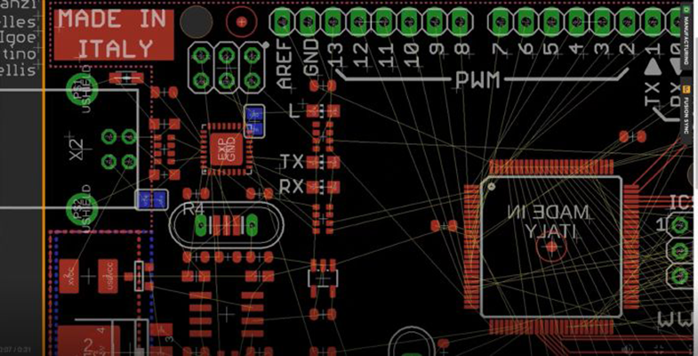
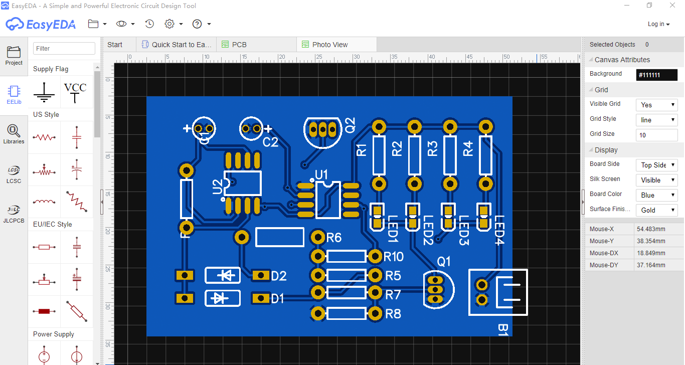
EasyEDA
EasyEDA is a Web-based EDA tool that can be opened in any HTML5 capable Web browser (preferably Chrome or Firefox)
 Key Features
- Quick online access to design tools by signing in to the website from any device.
- The tool runs on Windows, Linux, and macOS.
- Includes a wide variety of component libraries (more than 1 million parts) and the LCSC catalogs, featuring more than 200,000 parts with pricing and stock availability details.
- Includes library of 3D component symbols in the Schematic Symbol Wizard that can be used for schematic capture.
- In layout, auto-routing is available along with a limited 3D modeling feature.
- The cloud-based online working feature enables multiple users to work on the same project simultaneously.
- ‘Image to shape conversion’ is a unique feature that allows users to import an image and convert it to a custom shape by setting some required parameters.
Advantages of EasyEDA tool
- Team members can collaborate using this cloud-based online tool and improve overall productivity.
- No software download is required and hence can be used for quicker designs in stringent timeline projects.
Disadvantages of EasyEDA tool:
- Not an ideal option for complex designs.
- The requirement of a stable network connection for smooth usage of the tool can be a drawback.
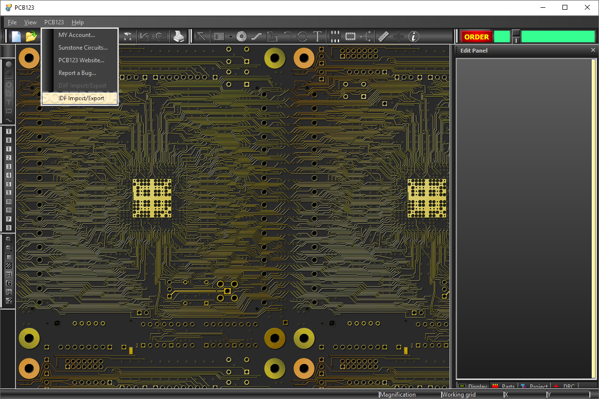
PCB123
PCB123 is a full-featured EDA tool from Sunstone Circuits with a focus on fast and accurate circuit design.
 Key Features
- Includes a complete suite for schematic capture, physical layout, BOM management, and real-time design rule checking.
- It is Windows-based software.
- Built-in, ‘Snap EDA online parts library’ provides access to over 750,000 predefined parts.
- 3D rendering view helps visualize the 3D circuit board and assists in inspecting placement, component pads, traces, etc.
- A Real-time Bill of Materials (BoM) is available as the schematic and layout tools operate in sync.
- Direct access to a fab shop that assures your robust circuit board manufacturing.
- Possible expansion of the tool for individual requirements, as it can access the PCB123 database.
Advantages of PCB123 tool:
- The tool supports advanced features like DRC and DFM to ensure a reliable circuit design.
- Ample technical support on tool usage and quick assistance for board production is a great advantage of this tool.
Disadvantages of PCB123 tool:
- The steep learning curve may be difficult for beginners to use the tool.
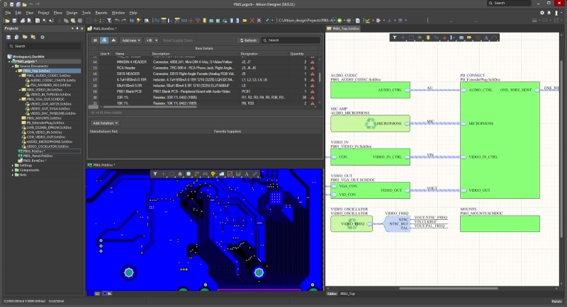
Altium Circuit Maker
Circuit Maker is a schematic and PCB Design software built upon Altium Designer technology.
 Key Features
- Built on a community library with lakhs of components backed by Octopart database.
- It is Windows-based software.
- Provides design capacity of up to 16 signal and 16 plane layers with no PCB dimension constraints.
- Easy placement of components just by searching manufacturing part numbers or vital parameters.
- Share and Collaborate work within a team to enhance overall productivity. Any edits or modifications done are dynamically updated and visible to all.
- Altium Native 3D” technology enables a 3D view of the PCB, and hence you can inspect for any overlays or component clearance violations.
- Push-N-Shove routing capabilities are a huge advantage enabling interactive routing, which can even route differential signals effectively.
- Provides complex multi-sheet designs with hierarchical design blocks. You can generate SmartPDF outputs of your project also.
Advantages of Circuit Maker:
- The tool provides DRC and DFM validated outputs necessary for professional manufacturing of the circuit design.
- The exclusive Situs topological auto-router is an advanced feature that is available in this free PCB design tool. This enables efficient auto-routing of complex circuits and is a great advantage.
Disadvantages of Circuit Maker:
- Available only on Windows OS and can run on Ubuntu with limitations.
- Doesn’t support offline saving of the design resource.
In the PCB Industry, production manufactures may choose a paid EDA tool having several sophisticated features. But some of the free PCB design tools discussed above are also capable of providing production-grade outputs. Start-up companies can try out tools like ‘Circuit Maker’ for high-quality PCB Manufacturing. Those new to the domain can work on the ‘KiCad’ tool as it’s very simple to understand. Finally, the choice of PCB Design tool depends on various criteria like software operating platform, support from the vendor, and the expertise of the PCB Engineer.
About the Author
Ken works as Sales Engineer at Technotronix, a PCB Manufacturing and assembly company. He brings 15 years of experience in Print Circuit Board Sales and Technical client Service. Feel free to get in touch with him on Twitter.