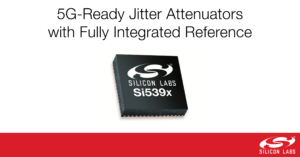
 Silicon Labs has expanded its family of Si539x jitter attenuators with new device options featuring a fully integrated reference, enhancing system reliability and performance while simplifying PCB layout in high-speed networking designs. The new Si539x jitter attenuators are purpose-built to address the demanding reference clock requirements of 100/200/400/600/800G designs, providing more than 40 percent margin to the stringent jitter requirements of 56G PAM-4 SerDes used in state-of-the-art Ethernet switch SoCs, PHYs, FPGAs and ASICs, while providing a solution that is future-proofed for emerging 112G SerDes designs.
The new Si539x jitter attenuators integrate a highly reliable crystal that has been fully tested over temperature and pre-screened for activity dips. The Si539x devices have been fully qualified over a broad range of reliability tests including shock, vibration, temperature cycling and crystal aging. The tightly specified crystal and innovative device construction reduce crystal sensitivity to temperature changes caused by system fans, leading to more consistent, reliable operation.
The integrated reference device construction provides higher immunity to acoustic emissions (AE) than external crystal-based designs. AE is the radiation of noise waves that occurs when a printed circuit board (PCB) is subject to temperature gradients or external mechanical forces that cause micro-cracks or plastic deformation in the PCB assembly. Unlike a discrete crystal that suffers from greater frequency error due to AE, the Si539x device’s innovative package construction isolates and protects the crystal from AE noise, ensuring reliable operation and consistent frequency response over time.
Customers designing high-port-count optical and Ethernet line cards place a premium on reducing overall board space. By using a jitter attenuator with an integrated reference, developers can minimize the PCB footprint by more than 35 percent. As an added benefit, an integrated reference eliminates the need for the keep-out area under the crystal, enabling denser clock routing around the device and further simplifying PCB layout.
The Si539x devices generate any combination of frequencies from 100 Hz to 1028 MHz on up to 12 differential clock outputs, eliminating the need for standalone clock generators and clock buffers. These benefits enable “clock-tree-on-a-chip” clocking while eliminating the additive jitter associated with discrete clock tree solutions.
Samples and production quantities of the new Si539x jitter attenuators are available now. Silicon Labs offers a wide range of evaluation boards (EVBs), priced at $299 each (USD MSRP), for Si539x devices with internal or external references. The EVBs enable customers to move quickly from device configuration to detailed performance evaluation, and they work seamlessly with ClockBuilder Pro, enabling developers to quickly develop custom configurations and measure performance.


Leave a Reply
You must be logged in to post a comment.