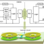
I am principally an analog designer who also designs custom ICs, but I also get involved in microcontrollers, and CPLD/FPGA design when necessary, which is quite often. Some applications are often clearly digital or analog, but others are not so clear. Which approach you take is likely to depend on your skill-set. A digital engineer might use a large DSP and digitize any signals as soon as possible and perform any filtering and processing in software. An analog engineer may avoid the digital domain except where necessary. But which is the “best”? That depends on your requirements and hence the definition of “best.”
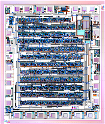
With IC design there was a rule of thumb I came across many years ago that digital takes up 40 times the area of analog. I never found any comparative results to substantiate the claim though. Certainly, the analog sections of mixed-signal ICs I worked on were considerably smaller than the digital circuitry but then the analog and digital sections were doing different jobs, so it isn’t the comparison I wanted. In the IC below, the regular patterning of the digital circuitry can be seen whereas the analog is mostly in the top right-hand corner and between the pads. However, it doesn’t prove the theory.
To compare digital with analog, you would need to do a design in each for the same application. To decide the “best” route you would need to define your criteria. Size, cost, and power consumption are three obvious attributes to consider. Product lifetime could be another – basic analog components are more likely to still be around in 20 years than a specialist digital component, allowing continued production and maintenance. Quantity is important because a custom IC is only likely to be economical in large volumes.
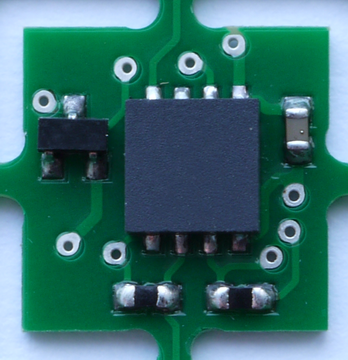
The closest I have come to a direct comparison of digital versus analog was a redesign of a product from over 20 years ago. The original design used a custom analog IC with unpackaged die to keep the size as small as possible (one of the requirements). The overall circuit size, including three essential external components, was 25mm2. The newer, digital design, used a microcontroller to perform the same function and required 64mm2 so was more than twice the size. This increase in size was anticipated, and some of the extra size was to accommodate the extra components — 7 in addition to the microcontroller compared to only 3 in addition to the custom IC with the analog approach. The microcontroller itself takes up a fair amount of the extra space – a 3x3mm DFN compared to a 1.2 x 1.35mm dice, although the dice does need space around for bond wires.
The performance was similar. A wider dynamic range was possible with the microcontroller and operating current was lower at around 3µA compared to 5µA with the custom IC. However, a newer custom IC design reduced the operating current to less than 2µA, so the microcontroller improvement was comparing an old IC design with a newer microcontroller one. Costs are difficult to compare exactly due to additional non-recurring engineering (NRE) charges for developing a custom IC and the different manufacturing companies required for chip-on-board manufacture of the custom IC board compared to assembling a conventional PCB. You also need to include the cost of programming the microcontroller in the calculations. Overall, the costs were fairly similar.
The main problem with the comparison was that the two designs were different and 20 years apart. The custom IC was mainly chosen initially to meet size constraints. At the time, a discrete analog or microcontroller solution would have never met the size or current consumption requirement. A digital or mixed signal custom IC approach could have been chosen but the higher NRE charge was out of the budget at the time. The newer microcontroller solution took advantage of the improvements in digital technology to add more features to the product that would not be possible with a pure analog solution. Extra space was created in the product to accommodate the larger size that was anticipated.
PCB layout of custom IC version – 25mm2 for the full circuit:
This example is a comparison between a modern digital (microcontroller) design and a 20-year-old custom analog IC design (which is still in production) rather than a discrete analog design. A discrete analog design would have been impossible with the size constraints. In each case, the solutions are “extreme.” In the case of the microcontroller, everything possible was done with the microcontroller to avoid extra components (although a few were required). In the case of the custom IC, digital circuitry was not needed and the external components could be reduced to just three.
As wafer sizes have increased and device geometries have shrunk, the custom IC approach probably wouldn’t make sense for this product anymore. It would require annual quantities of 50,000 or more to be economical whereas 20 years ago with 4″ wafers and larger geometries, less than 20,000 chips per year were economical.
With severe size constraints, it is useful to take an estimate of the parts required and see if they will fit in the available space. In this case, a quick check was made of the bare minimum solution for a microcontroller with five external components and a six pin SOT package rather than an eight pin DFN. They still wouldn’t fit in the available space, so the decision to make more space available while increasing the microcontroller size and hence adding more options was taken.


Leave a Reply
You must be logged in to post a comment.