The field-effect transistor (FET) in one form or another has largely superseded the earlier bipolar junction transistor (BJT). Both can do amplification, oscillation, and switching, but the methods in getting there are quite different as are the input and output impedances.
First, by way of background, we’ll look back at the BJT. It contains three layers of doped semiconductor, therefore two junctions. In the most common configuration, the BJT consists of two N-type layers with a P-type layer between them, so it is called an NPN transistor. The less-used PNP works the same, but with all polarities reversed. Each of the layers has a permanently affixed lead.
The most common BJT configuration is as a current amplifier where a small current applied to the base controls a larger current that flows between the collector and the emitter. The NPN-type BJT conforms to these basic principles: First, the collector is positive with respect to the emitter. Second, the base-emitter and base-collector circuits function as separate diodes. In operation, the base-emitter junction is forward biased, so it conducts. The base-collector junction is reverse biased, so it does not conduct. However, current flows between these two points due to transistor action.
In a FET, amount of current through a channel connecting source and drain is controlled by variations in an electrical field present at the gate. Because the FET has a gate with a minute amount of mass, the electrical field associated with it is accompanied by a current close to zero. As a consequence, the FET input impedance is high so the preceding stage is not appreciably loaded.
Like BJTs, FETs come in two varieties with opposite polarities: N-channel FETs in which conduction is by electrons, and P-channel FETs in which conduction is by holes. A hole is simply the absence of an electron, but it may be thought of as a positive, charge-carrying particle. Also, we must be aware that FETs can have two types of gates. There are junction FETs (JFETs) and metal-oxide-semiconductor FETs (MOSFETs). Also, there are depletion mode and enhancement mode FETs with two different types of channel doping.
The N-channel enhancement mode MOSFET is the semiconductor of choice in a great variety of circuits. Ordinarily, the drain is positive with respect to the source just as in BJTs the collector is more positive than the emitter. When the gate (analogous to base) is more positive than the source, current flows from drain to source. This makes possible amplification, oscillation, and switching.
And just as BJTs exist as NPN and PNP devices, MOSFETs come as N-channel and P-channel versions. The charge carriers in a P-channel MOSFET, however, are holes with less mobility than electrons, making for reduced capabilities. For this reason, the N-channel MOSFET is more widely used.
The MOSFET gate is strongly insulated from the source-to-drain channel. The glass layer that does not permit current to flow from the gate regardless of the device’s electrical status nevertheless is transparent to the electrical field radiated by the gate just as glass, an electrical insulator, is a near-perfect medium for light.
The downside is that MOSFETs are instantly destroyed by any slight static electricity that may arise in handling. MOSFETs generally ship in anti-static packaging, often with the leads shorted out to prevent static charge differential. Technicians wear grounded anti-static bracelets when handling these devices or printed circuit boards containing them.
N-channel MOSFETs are non-conducting with zero or negative gate bias. They become conductive when the gate is made more positive than the source. They are, therefore, enhancement mode devices. If, however, in the manufacturing process the channel is doped so it conducts with zero gate bias, the FET is a depletion mode device. Since JFETs have gate-to-channel diode behavior, they operate only when reverse biased, so they exist only in depletion mode. The MOSFET may exist in either mode because the gate is truly insulated from the channel. However, most MOSFETs are made in the enhancement mode.
To summarize, JFETs are depletion-mode devices and MOSFETs are mostly enhancement-mode devices. Both subspecies are available in N-channel and P-channel models.
There is an interesting quality of a MOSFET that results from its high gate capacitance which, in turn, arises from the extremely thin glass insulating barrier with its high dielectric constant. This behavior, which is unique among active devices, is that once turned on, it remains in that state even if the input circuit disconnects! This is because of the gate-to-channel capacitance in conjunction with the high input impedance, which can exceed 1014 Ω.
Functional MOSFETs always exhibit this charge retention, and the behavior can be exploited to check the device using the multimeter in the diode test mode. First, touch a well-grounded metal surface to drain any static charge that could destroy the device being tested.
Then, begin by connecting the channel through source or drain to the negative lead of the multimeter. (Throughout this test, handle the MOSFET by holding the case or tab.) Next, touch the meter’s positive lead to the gate. Then connect the positive lead to the source. If the device is good, expect to see a low reading. The meter will charge the MOSFET and it should remain charged for at least an hour, unless it is intentionally discharged, as in the next portion of this test.
With the meter still connected as above, touch your finger to gate and drain or gate and source. This will discharge the MOSFET, and the meter will now read high, indicating that the device is non-conducting and good.
Devices that pass the multimeter tests will be free of some common MOSFET failure modes, but the test is not absolutely definitive.
A laboratory-grade transistor test instrument performs a true dynamic test. It applies signal and bias voltages at the inputs and analyzes the output. Expect to pay a high price for this instrument.
An oscilloscoope in the XY triggered mode displays Lissajous patterns which can be used to determine the status of a transistor. These tests take place using an octopus, which eliminates problems associated with testing components that are in a circuit board. To do an accurate multimeter test, all but one lead must be disconnected. This procedure involves soldering/desoldering operations, which can damage the sensitive MOSFET because of heat and circulating currents. (Even the best soldering techniques are problematic with modern downsized components and board densities.)
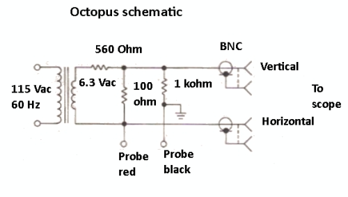
An octopus produces a Lissajous pattern that reveals the condition of the component under test.
These problems are avoided using the octopus, which can be field assembled using a 6.3-V filament transformer and three resistors. It is easy to build an octopus. The only component priced over a dollar is the 6.3-V filament transformer, which can be salvaged from old tube-type equipment. A metal enclosure (Be sure to ground it!), power light and switch will round out the project. An old analog oscilloscope with vertical and horizontal inputs, available from auction sites for under $100, would be the basis for a valuable transistor test instrument.
There is a moderate learning curve involved in interpreting the Lissajous patterns. To operate this user-built instrument, connect the vertical output of the octopus to the oscilloscope vertical input and the horizontal output of the octopus to the oscilloscope horizontal input. If the component is part of a PCB, remove power and discharge any lingering voltages. If the PCB or chassis is grounded, connect the black test lead to the component’s grounded terminal or lead.
The red and black octopus leads can be connected to component terminals and these patterns are displayed:
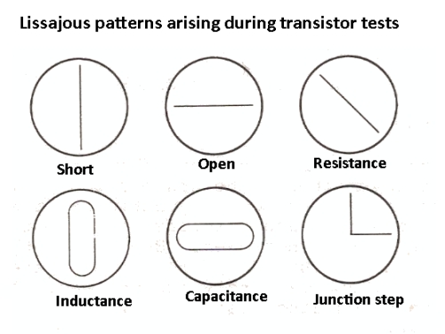
Typical Lissajous patterns. A good junction displays as a right angle. Larger angles indicate poor junction performance. 120° is questionable and 150° is non-functional.
A good way to get a feel for using this instrument to evaluate transistors (and a wide variety of other components) is to try it on known good and bad devices and sketch the resultant Lissajous patterns.




Leave a Reply
You must be logged in to post a comment.