Researcher say the deep-depletion regime of bulk-boron-doped wide band gap semiconductors could be an avenue toward power MOSFETs able to handle large voltages and high temperatures.
A group with members based in France, the UK and Japan applied the technique to diamond-based MOSFETs. But they say a similar scheme would work in other wide-band-gap semiconductors. They have used the idea to produce simple diamond MOSFET structures from single boron-doped epilayer stacks. This new method boosts a diamond-based MOSFET’s hole channel carrier mobility by an order of magnitude.
The group apparently thinks their approach is promising enough to commercialize. They have formed a start-up called DiamFab to bring the idea to market.
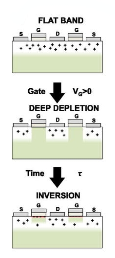
The three different conduction regimes: flatband regime, deep depletion regime, and inversion regime.
In a typical MOSFET, an oxide layer and a metal gate sit on top of a semiconductor material. Applying a voltage to the metal gate modulates the carrier density, and thus the conductivity, of the channel region under the gate. In the past, it has been tough to get enough charge carriers into the channel. The on-state current of a MOSFET strongly depends on the channel mobility which is often sensitive to roughness and defect states at the oxide-diamond interface where unwanted carrier scattering arises.
The deep-depletion concept is said to overcome the carrier scattering problem. To build their MOSFET, the researchers deposited a layer of aluminum oxide (Al2O3) at 380°C over an oxygen-terminated thick diamond epitaxial layer. They created holes in the diamond layer by incorporating boron atoms. Boron has one less valence electron than carbon, so its presence leaves a missing electron which acts like the addition of a positive charge, or hole. The resulting layer of material functioned as a thick conducting hole channel.
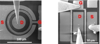
SEM images of the diamond-based MOSFETs.
Applying a voltage switches the resulting transistor from on to off because the voltage repels and deplets the holes to form the deep depletion region. The idea won’t work in silicon-based transistors because this voltage would form an inversion layer and the transistor would not have turned off. The group says the special properties of diamond, and in particular its large band gap, suppressed formation of the inversion layer and made operation in the deep depletion regime possible.
The group described their work in Applied Physics Letters.


Leave a Reply
You must be logged in to post a comment.