Designers are now investigating exotic power supply topologies in a quest for efficient operation.
RICK BARNETT,
ED FONTANA,
JIM MONTGOMERY,
EMBEDDED SOLUTIONS,
GE INDUSTRIAL SOLUTIONS BUSINESS
IT’S no secret that power converters increasingly emphasize energy efficiency. For example, 115-Vac computer power supplies must exhibit a 94% energy efficiency at 50% of their rated load to receive an 80 Plus Titanium rating; 230-Vac supplies must hit 96% at half their rated load to get the designation. For external power supplies (as used by laptops, tablets, and so forth), the Dept. of Energy recently came out with Level VI energy efficiency standards mandating active-mode efficiencies in the 86 to 88% range from most output powers.
A generally understood maxim is that for power supplies to get denser, they must also get more efficient. That works up to a point. Then you reach a point where incremental increases in efficiency come only at great cost and effort, or alternately, you must give relief on one to get the other.
As a generality, there’s a brick wall in 48-V power at around 50 W/in3 and 97% efficiency. Designing a power supply that can blow past the brick wall by increasing both density and efficiency is the goal. But it is extremely difficult and only comes with great cost (more expensive components and greater R&D costs).
One truth we have learned is that we have reached the brick wall and it’s not moving. The only way beyond it is to look at circuits differently. So we look at what the circuits are made of and how they behave — Like using super magnetic materials, or ultra-fast switching semiconductors, or applying switching logic (firmware) to the internal functions of the power supply. Only by looking at circuits from a fresh perspective do we find ways around the brick wall.
Additionally, customers sometimes bring requirements that call for specific operating ranges falling outside what the electronics will support. So the designer may be faced with falling back to an older topology (lower density and lower efficiency) to support the customer criteria.
There is an alternative topology called resonant LLC that takes the bolder approach of looking again at ways in which the electronic circuitry can be manipulated to “have it all.” The goal is to retain maximum efficiency, maximum density and also provide a flexible and resilient power supply that can operate over a wide range of conditions. That is extremely hard to do, yet it is what we have done.
To understand the approach, first consider that one way switch-mode supplies boost efficiency is by becoming smaller. The main way they get smaller is by using higher operating frequencies to reduce the size of the power magnetics and LC components in the output. However, going to higher switching frequencies leads to higher transistor switching losses at turn-off and turn-on when the supply works with conventional square-wave current. The turn-on losses arise from charging the transistor output capacitances and can be appreciable at frequencies over about 1 MHz.
The overlap of falling current and rising collector voltage at turn-off brings a spike of dissipation during turn-off. This effect is more problematic as switching frequencies rise because the more frequent spikes lead to higher average transistor dissipation.
A switching topology called a resonant converter was developed to reduce the amount of energy dissipated in the switching transistor during turn-on and turn-off. Resonant converters associate an LC circuit with the switching transistor to change its current waveform from square to sinusoidal. The switching transistor is timed to turn on and off at the zero crossings of the current sine wave. Thus there is no overlap of falling current and rising voltage at the turn-off, nor rising current and falling voltage at turn-on.
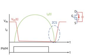
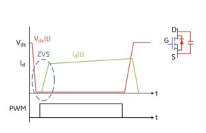
Waveforms depicting the drain current Id and drain-source voltage of the MOSFET switching elements show the position in time of zero-voltage switching and zero-current switching.
Circuits which turn on and off at zero current are known as zero-current switching (ZCS) types. A point to note, however, is that there can be switching losses at turn-on in a ZCS though there is no overlap of rising voltage and falling current at the zero-crossing of the current sine wave. Zero-voltage switches (ZVS) cope with this difficulty by ensuring the transistor output capacitance is part of a resonant LC circuit. The voltage or energy stored on the capacitor when the transistor is off gets stored as current or energy in the inductor of the resonant circuit. Later in the cycle, the energy gets returned without loss to the power supply bus.
Some switching topologies employ what’s called quasi-resonant operation. This refers to switching done in such a way that the transistor turns on when the voltage across it is at a minimum but not zero. The term soft switching is frequently used to refer generally to resonant converter schemes for both ZVS and ZCS as well as to quasi-resonant techniques.
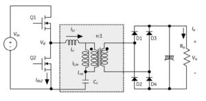
Typical schematic for an LLC converter. The LLC portion of the circuit is made up by Lr, Lm, and Cr . The layout of the LLC is quite close to that of a series-resonant LC converter. An LC converter might also incorporate a second inductor in the form of a transformer, but the inductance of the second inductor in the LC converter would be set so that the resulting resonance would be far away from the converter operating frequencies. This converter is also shown with a passive diode rectifier bridge in the secondary. Super-efficient LLC converters more typically use MOSFET bridge elements that are actively switched to less power dissipates in the switches themselves. Not shown in this schematic is the feedback network used to adjust the width of the pulse modulation in response to changes in load.
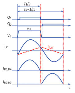
Current flow through the two inductors during the switching sequence of the two switching transistors Q1 and Q2. The top waveforms are the turn-on pulses to the two switching transistors respectively with the resulting voltage at point Vd in the accompanying schematic. The currents through the two inductors ILr and ILm respond as shown, resulting in the current flows though diode bridge legs D1 and D4, and D2 and D3.
Approaches for soft-switched resonant converters have been around for years, but their realization has sometimes brought mixed results. The problem is it can be tricky to design a circuit able to properly time the turn-on and turn-off of the transistor, typically a field effect transistor. Under different line and load conditions the operating points can shift considerably, and the timing of the turn-on and turn-off must change. But recently, improvements in digital signal processors have enabled more flexible control schemes, making the use of such methods easier.
One specific ZVS/ZCS approach employs an LLC configuration which uses two inductors in a series-parallel combination with a capacitor. An ac-dc converter using an LLC topology can reach energy efficiencies approaching 96.5%.
The operation of an LLC converter is often explained in terms of a series-resonant LC circuit combined in series with an additional inductor. The second inductor is in parallel with the load.
The explanation generally begins by first considering the series-resonant circuit by itself. In a general series-resonant circuit, the impedance of the resonant network hits a minimum at the resonant frequency. Because the converter is controlled through frequency modulation, the impedance of the resonant circuit changes with switching frequency which, in turn, changes in response to load changes. A decrease in load current, for example, tends to decrease the output voltage. A feedback circuit will sense the decrease and move the switching frequency of the converter toward resonance such that more voltage drops across the load. Similarly, a drop in load current results in converter frequency moving away from resonance so more voltage drops across the LC tank circuit.
A point to note about the series-resonant converter is that the current only lags the applied voltage above resonance. An examination of the phase plot for this circuit reveals that below resonance, phase is below 0°, so the network will be capacitive to the input source. This means the switching transistors won’t operate as zero-voltage switches below this series-resonance point.
One drawback of a series resonant converter is that circuit Q drops as the load decreases. So switching frequency must rise significantly to keep the output regulated. This need for a large frequency change is difficult to implement in practical circuits. In this regard, the LLC resonant converter is designed to overcome the disadvantages of the series resonant converter.
The second inductor in the LLC converter is frequently comprised of the leakage inductance of the primary of a transformer. The load resistance is reflected back into the primary circuit through the turns ratio of the transformer. This action effectively puts the load in parallel with the second inductor.
The leakage inductance value of the transformer is such that it affects the resonance of the LLC components. Specifically, it has the effect of creating a second resonance frequency that differs from that of the series-resonant LC. An examination of the gain and phase plots for the resulting LLC circuit reveals that soft switching is possible only when the LLC circuit operates between the upper and lower resonance frequencies.
More specifically, it is possible to show from the operational parameters under various loads that the most advantageous operation point for the LLC converter is at the upper resonance point. At this point, there is little frequency change over an extremely wide range of loads. In fact, the LLC converter can keep the output voltage regulated even when there is no load.
Energy efficiencies in any converter topology can improve through use of an FET synchronous rectifier bridge on the secondary side rather than a diode bridge. Use of an active switching element such as a FET or MOSFET boosts efficiency because these devices have a constant and low resistance when conducting, known as on-resistance (RDS(on)). The on-resistance can be 10 mΩ or even lower. The voltage drop across the transistor is then much lower than would be the case for a diode. Thus there is less power dissipated in the switching elements themselves.
All in all, converters using an LLC topology along with synchronous rectification have been shown to work at energy efficiencies of about 96%. Their ability to operate efficiently across a broad range of power demands and in harsh conditions makes them good candidates for handling industrial applications.