It can be tough to harvest energy from innovative IoT devices such as thermoelectric generators built into clothing. A new kind of MOSFET is designed to work with the super-low voltages involved.
Robert Chao | Advanced Linear Devices Inc.
Energy harvesting devices make headlines because they are thought to be important for internet-of-things applications. As an example, consider a flexible fabric capable of generating power from body heat. According to researchers in China and Australia who recently described the new material in the journal Scientific Reports, it can generate 4.3 mV into a large impedance when exposed to a temperature difference of 75.2°K.
However, the hype surrounding such developments rarely mention the problems involved in working with such low voltages and the minuscule amount of energy being harvested. The difficulty with energy harvesters such as the fabric mentioned above is that the voltages generated are close to the gate-threshold voltage of ordinary transistors. It can be tricky to manipulate harvested energy when it exists at such low voltages.
Consequently, there has been a need for semiconductor devices able to function with low levels of input energy. One development in that category is a zero-gate threshold voltage P-Channel MOSFET array. Called the ALD310700A/ALD310700, it is intended for use in small-signal precision applications involving zero threshold voltage. The array targets designs requiring operating voltages below a half volt. Notable device features include a minimum operating voltage of less than 0.2 V, minimum operating current of less than 1 nA, and matched and tracked temperature qualities.
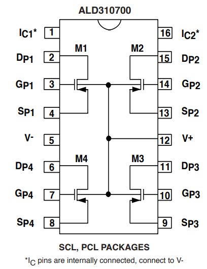
The ALD310700A/ALD310700 high-precision P-Channel MOSFET arrays are available in a quad version with a block diagram as depicted here.
Zero-threshold MOSFETs are a special case of a family of MOSFETs called EPAD (Electrically Programmable Analog Device) where the individual threshold voltage of each MOSFET is fixed at zero. Here, use of EPAD technology leads to low-voltage switching with sharp turn-off and low leakage qualities resembling those of conventional MOSFETs.
In these zero-threshold transistor arrays, the zero-threshold voltage is defined as Ids = 1 µA at Vds = 0.1 V when the gate voltage Vgs = 0.0 V. Technically, the zero-threshold devices are enhancement-mode transistors when operated above threshold voltage and current level (greater than 0.0 V and 1 µA). However, these devices can also be used as normally-on MOSFETs because they conduct a current and behave like a fixed-resistor even when the gate voltage is at 0.0 V. A modulating signal voltage at the gate can adjust the drain current, even to negative-gate voltage levels, down to a subthreshold voltage level of about -0.4 V, at which point the transistor is completely off.
A zero-threshold MOSFET reduces or eliminates input-to-output voltage level shift in circuits where the signal is referenced to ground or V+. This feature can significantly reduce output signal level shift from that of the input and enhances operating signal range, especially for low operating voltage environments. With zero-threshold devices, an analog circuit with multiple stages can be constructed to operate at extremely low power supply or bias voltage levels.
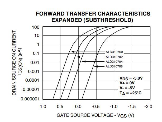
A view of the forward transfer curves for the ALD310700A/ALD310700 shoes how the devices can help in the creation of circuit designs with low operating voltages, as when operating from power supplies of less than +0.5 V, where the circuits operate below the threshold voltage. This feature also enhances input/output signal operating ranges, especially in environments characterized by low operating voltages.
The EPAD technology upon which the zero-threshold MOSFET is based employs a CMOS MOSFET whose threshold voltage and on-resistance characteristics can be electrically programmed to a precise level. Once programmed, the set parameters are indefinitely stored within the device even after power is removed. This technology makes use of a floating gate structure which can be precision-trimmed to produce tightly controlled transistor electrical qualities.
In general, EPAD devices can serve as functional trimmer pot substitutes in conjunction with external fixed resistor(s). The primary function of an EPAD MOSFET is as a high-precision, high-stability MOSFET that displays a special family of voltage-versus-current curves. Originally, EPAD MOSFETs were used as trimmers where the on-resistance of the MOSFET could be precisely set to replace a trimmer potentiometer. But many other uses have emerged. An EPAD MOSFET is actually a CMOS IC, and it has some general limitations of typical CMOS devices such as a maximum voltage rating of 10 V. It is sensitive to electrostatic discharge and has an NMOS MOSFET device output.
Basics of low-voltage operation
Low-voltage systems — namely those operating at 5 V, 3.3 V or less — typically require MOSFETs that have threshold voltage of 1 V or less. The threshold, or turn-on, voltage of the MOSFET is a voltage below which the MOSFET conduction channel rapidly turns off. For analog designs, this threshold voltage directly affects the operating signal voltage range and the operating bias current levels.

The gate threshold voltage VGS(th) on the ALD310700A/ALD310700 is set precisely at 0.00 ±0.02 V, featuring a typical offset voltage of only ±0.001 V (1 mV). As the MOSFETSs are on the same IC, they also exhibit excellent temperature tracking. The operating current level varies exponentially with gate bias voltage at or below the gate threshold voltage (subthreshold region). The circuit can also be biased and operated in the subthreshold region with nanoamps of bias current and nanowatts of power dissipation. These qualities make the MOSFETs versatile design components for a broad range of precision analog applications such as basic building blocks in current mirrors and differential amplifiers.
At or below threshold voltage, an EPAD MOSFET exhibits a turnoff characteristic in an operating region called the subthreshold region. This is when the EPAD MOSFET conduction channel rapidly turns off as a function of diminishing applied gate voltage. The conduction channel induced by the gate voltage on the gate electrode drops exponentially and causes the drain current to fall exponentially.
However, the conduction channel does not shut off abruptly with diminishing gate voltage. Rather, it decreases at a fixed rate of approximately 116 mV/decade of drain current reduction. Thus, if the threshold voltage is +0.20 V, for example, the drain current is 1 µA at VGS = +0.20 V. At VGS = +0.09 V, the drain current would drop to 0.1 µA. Extrapolating from this, the drain current is 0.01 µA (10 nA) at VGS = -0.03 V, 1 nA at VGS = -0.14 V, and so forth. This subthreshold characteristic extends all the way down to current levels below 1 nA and is limited by other currents such as that for junction leakage. At a drain current to be declared “zero current” by the user, the corresponding VGS voltage can be estimated. Note that using the above example, with VGS(th) = +0.20 V, the drain current still hovers around 20 nA when the gate is at zero volts, or ground.
When supply voltages drop, the power consumption of a given load resistor drops as the square of the supply voltage. So one of the benefits in reducing supply voltage is to reduce power consumption. However, a decreasing power supply voltage and power consumption go hand-in-hand with a diminishing useful ac bandwidth. Simultaneously, noise has a bigger impact on low-level signals. So circuit designers must make the necessary trade-offs and adjustments in any given circuit design and bias the circuit accordingly
One other key benefit of using matched-pair EPAD MOSFETs is to maintain temperature tracking. In general, for EPAD MOSFET matched pair devices, one device of the matched pair has gate leakage currents, junction temperature effects, and drain current temperature coefficient as a function of bias voltage that cancel out similar effects of the other device. Temperature stability can be further enhanced by biasing the matched-pairs at the Zero Tempco (ZTC) point, though that could require special considerations for circuit configurations and power consumption.


Leave a Reply
You must be logged in to post a comment.