It’s a very common challenge in circuits to need to convert an available DC source to a lower or higher voltage. For the high-to-low conversion, one option to use a low dropout regulator (LDO), but how to easily transform a lower voltage into a higher one?
For AC voltages, the answer is well-known: use a transformer, as has been done for well over 100 years. Yet as even every first-year electrical engineering student knows, you can’t use a transformer with DC. The obvious approach, then, is to “chop” the low-voltage DC using an oscillator of some sort, pass the chopped, AC-like waveform through a step-up transformer, and then rectify and filter it at the secondary-side output. This approach can be very successful, and enhanced versions of it are the basis for switching power supplies, used to both increase (boost) and decrease (buck) the voltage between a DC source and a supply rail.
What are the drawbacks of this approach?
The key issue is the need for the transformer, an inductive component which is a relatively large and costly component compared to the rest of the power-conversion circuitry it supports. While some power converters actually prefer or even mandate a transformer due to the inherent galvanic isolation it provides, that benefit is often not needed in low-voltage circuits or localized subcircuits. A transformer-based design’s performance and cost are more suited for DC/DC converters above about 1 to 5 A output, but it is generally not an attractive solution at the low end below a few hundred mA.
What’s the better alternative?
Circuit designers have developed a topology called the charge pump, which is actually difficult to implement with discrete components, but is very IC-friendly. The charge pump uses capacitors as the energy-storage element.
In the basic execution of this power-conversion technique, current (charge) is alternately switched and directed between two capacitors arranged so the circuit output is twice the input, and thus functioning as a voltage-doubling boost converter. For these reasons, the charge-pump converter is also known as a switched-capacitor design.
[Note that a variation of the charge-pump voltage converter is used in phase lock loops (PLL); but that application and its attributes are beyond this power-related discussion.]How does the charge-pump voltage-doubler work?
How is this voltage-doubling boost accomplished? It all starts with a fundamental principle of physics: charge flowing back and forth in a closed circuit is not “lost,” but instead can be transferred via switching between charge-storage elements. In a charge-pump concept, diodes can be used to control the flow of current; in actual practice, the switches are usually switched MOSFETs, and the capacitors are external ceramic or electrolytic devices depending amount of capacitance needed.
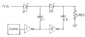
The operation, Figure 1, is a two-step charge-discharge cycle where capacitor C1 charges, then discharges into C2. First, the clock drives the output of inverter 1 low, so D1 is forward-biased, thus charging capacitor C1 to the supply voltage +Vdc; also, D2 is off.
Next, the clock drives the output of inverter 1 high, and the charge on C1 is now in series with +Vdc from inverter 1. As the output of inverter 2 is low, D2 becomes forward-biased and C2 charges to twice Vdc. The voltage thus seen across the load is 2 × Vdc, minus the diode forward-voltage drops and any losses in the inverters.
In practical designs using discrete components, Schottky diodes are usually used instead of conventional diodes because of their lower forward-voltage drop. However, IC-based charge pumps do not use diodes; instead, they use MOSFET switches with low on-resistance RDS(ON). Charge pump efficiency is fairly high, in the range of 90 to 95%.
Part 2 looks at some additional aspect of charge pumps, including their capacitors, non-doubling variations, internal and external clocks, filtering and regulation, and embedded charge pumps.


