• Skip to primary navigation
  • Skip to main content
  • Skip to primary sidebar
  • Skip to footer

Electrical Engineering News and Products

Electronics Engineering Resources, Articles, Forums, Tear Down Videos and Technical Electronics How-To's

  • Products / Components
    • Analog ICs
    • Battery Power
    • Connectors
    • Microcontrollers
    • Power Electronics
    • Sensors
    • Test and Measurement
    • Wire / Cable
  • Applications
    • 5G
    • Automotive/Transportation
    • EV Engineering
    • Industrial
    • IoT
    • Medical
    • Telecommunications
    • Wearables
    • Wireless
  • Learn
    • eBooks / Handbooks
    • EE Training Days
    • Tutorials
    • Learning Center
    • Tech Toolboxes
    • Webinars & Digital Events
  • Resources
    • White Papers
    • Educational Assets
    • Design Guide Library
    • Digital Issues
    • Engineering Diversity & Inclusion
    • LEAP Awards
    • Podcasts
    • DesignFast
  • Videos
    • EE Videos and Interviews
    • Teardown Videos
  • EE Forums
    • EDABoard.com
    • Electro-Tech-Online.com
  • Bill’s Blogs
  • Advertise
  • Subscribe

First On-Chip Nanoscale Optical Quantum Memory Developed

September 12, 2017 By California Institute of Technology

Artist’s representation of the quantum memory device. (Credit: Ella Maru Studio)

For the first time, an international team led by engineers at Caltech has developed a computer chip with nanoscale optical quantum memory.

Quantum memory stores information in a similar fashion to the way traditional computer memory does, but on individual quantum particles–in this case, photons of light. This allows it to take advantage of the peculiar features of quantum mechanics (such as superposition, in which a quantum element can exist in two distinct states simultaneously) to store data more efficiently and securely.

“Such a device is an essential component for the future development of optical quantum networks that could be used to transmit quantum information,” says Andrei Faraon (BS ’04), assistant professor of applied physics and materials science in the Division of Engineering and Applied Science at Caltech, and the corresponding author of a paper describing the new chip.

The study appeared online ahead of publication by Science magazine on August 31.

“This technology not only leads to extreme miniaturization of quantum memory devices, it also enables better control of the interactions between individual photons and atoms,” says Tian Zhong, lead author of the study and a Caltech postdoctoral scholar. Zhong is also an acting assistant professor of molecular engineering at the University of Chicago, where he will set up a laboratory to develop quantum photonic technologies in March 2018.

The use of individual photons to store and transmit data has long been a goal of engineers and physicists because of their potential to carry information reliably and securely. Because photons lack charge and mass, they can be transmitted across a fiber optic network with minimal interactions with other particles.

The new quantum memory chip is analogous to a traditional memory chip in a computer. Both store information in a binary code. With traditional memory, information is stored by flipping billions of tiny electronic switches either on or off, representing either a 1 or a 0. That 1 or 0 is known as a bit. By contrast, quantum memory stores information via the quantum properties of individual elementary particles (in this case, a light particle). A fundamental characteristic of those quantum properties–which include polarization and orbital angular momentum–is that they can exist in multiple states at the same time. This means that a quantum bit (known as a qubit) can represent a 1 and a 0 at the same time.

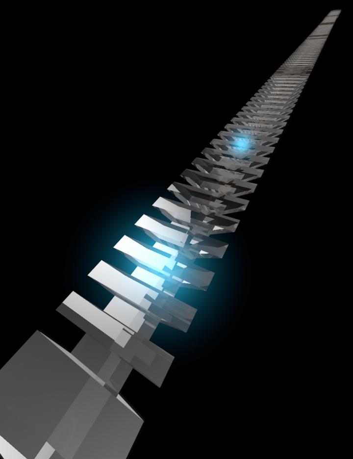
To store photons, Faraon’s team created memory modules using optical cavities made from crystals doped with rare-earth ions. Each memory module is like a miniature racetrack, measuring just 700 nanometers wide by 15 microns long–on the scale of a red blood cell. Each module was cooled to about 0.5 Kelvin–just above Absolute Zero (0 Kelvin, or -273.15 Celsius)–and then a heavily filtered laser pumped single photons into the modules. Each photon was absorbed efficiently by the rare-earth ions with the help of the cavity.

The photons were released 75 nanoseconds later, and checked to see whether they had faithfully retained the information recorded on them. Ninety-seven percent of the time, they had, Faraon says.

Next, the team plans to extend the time that the memory can store information, as well as its efficiency. To create a viable quantum network that sends information over hundreds of kilometers, the memory will need to accurately store data for at least one millisecond. The team also plans to work on ways to integrate the quantum memory into more complex circuits, taking the first steps toward deploying this technology in quantum networks.

You Might Also Like

Filed Under: Artificial intelligence

Primary Sidebar

EE Engineering Training Days

engineering

Featured Contributions

Integrating MEMS technology into next-gen vehicle safety features

Five challenges for developing next-generation ADAS and autonomous vehicles

Robust design for Variable Frequency Drives and starters

Meeting demand for hidden wearables via Schottky rectifiers

GaN reliability milestones break through the silicon ceiling

More Featured Contributions

EE Tech Toolbox

“ee
Tech Toolbox: 5G Technology
This Tech Toolbox covers the basics of 5G technology plus a story about how engineers designed and built a prototype DSL router mostly from old cellphone parts. Download this first 5G/wired/wireless communications Tech Toolbox to learn more!

EE Learning Center

EE Learning Center
“ee
EXPAND YOUR KNOWLEDGE AND STAY CONNECTED
Get the latest info on technologies, tools and strategies for EE professionals.
“bills
contribute

R&D World Podcasts

R&D 100 Episode 10
See More >

Sponsored Content

Designing for Serviceability: The Role of Interconnects in HVAC Maintenance

From Control Boards to Comfort: How Signal Integrity Drives HVAC Innovation

Built to Withstand: Sealing and Thermal Protection in HVAC Sub-Systems

Revolutionizing Manufacturing with Smart Factories

Smarter HVAC Starts at the Sub-System Level

Empowering aerospace E/E design and innovation through Siemens Xcelerator and Capital in the Cloud

More Sponsored Content >>

RSS Current EDABoard.com discussions

  • Industrial Relay Board Design for Motorcycle Use
  • Sendust vs Ferrite for SMPS
  • On/Off Slide Switch Reassembly Help
  • sim7090g
  • connector model question

RSS Current Electro-Tech-Online.com Discussions

  • using a RTC in SF basic
  • Is AI making embedded software developers more productive?
  • Wierd makita battery
  • ac current limiting
  • I Wanna build a robot
Search Millions of Parts from Thousands of Suppliers.

Search Now!
design fast globle

Footer

EE World Online

EE WORLD ONLINE NETWORK

  • 5G Technology World
  • Analog IC Tips
  • Battery Power Tips
  • Connector Tips
  • DesignFast
  • EDABoard Forums
  • Electro-Tech-Online Forums
  • Engineer's Garage
  • EV Engineering
  • Microcontroller Tips
  • Power Electronic Tips
  • Sensor Tips
  • Test and Measurement Tips

EE WORLD ONLINE

  • Subscribe to our newsletter
  • Teardown Videos
  • Advertise with us
  • Contact us
  • About Us

Copyright © 2025 · WTWH Media LLC and its licensors. All rights reserved.
The material on this site may not be reproduced, distributed, transmitted, cached or otherwise used, except with the prior written permission of WTWH Media.

Privacy Policy