 Lattice Semiconductor Corporation announced a Single Wire Aggregation (SWA) IP solution for reducing overall system size and BOM cost in industrial, consumer, and computing applications. The solution is a quick, easy, and innovative way for developers to use low power, small form factor Lattice FPGAs to dramatically reduce the number of board-to-board and component-to-component connectors in their embedded designs to increase reliability and reduce overall system footprint and cost.
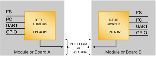
The connectors used to link circuit boards and modules in electronic systems are costly, take up valuable space in devices with tight form factors, and over time can degrade and negatively impact system reliability. Routing signals between multiple connectors on space-constrained circuit boards can create design challenges that increase overall time-to-market.
Featuring the extremely low power and small size Lattice iCE40 UltraPlus™ FPGA, the SWA solution provides the hardware and software developers require to implement a single wire interface capable of aggregating multiple common I/O (I2C, I2S, UART and GPIO) data streams between components and circuit boards in a system. Lattice currently offers the following aggregated I/O configurations in pre-configured bitstreams for fast application prototyping.
- Two I2S, an I2C peripheral, an I2C controller, and eight GPIO signals
- Six I2C controller and two GPIO signals
- One I2C controller and 12 GPIO signals
- Three I2C controller, two I2C peripheral, and 15 GPIO signals
- One I2S, one I2C controller, one I2C peripheral, and eight GPIO signals
Lattice customers requiring customized configurations can source them directly from Lattice technical support at no charge.
The board is available for purchase at $249.00 from Lattice’s online store.
