Integrating a wireless module and antenna into a system requires thought, making design tradeoffs, achieving certification, and testing in production.
When you embark on an IoT device design that uses wireless modules, you’ll face decisions that include which bands to use, the type of antenna (make or buy), and the tests needed for both qualification and in manufacturing. Your device’s intended use case— be it medical, industrial, asset tracking, or sensing, to name a few — factor into design decisions.
In addition to use cases, product specifications, expected performance, and selected carriers will greatly influence your design and technical choices. For example, the number of bands and the carrier requirements of your product will define 90% of the antenna selection and the work needed to integrate the antenna into the product. The number of bands and the frequencies they occupy have a direct effect on the antenna design, antenna tuner, and matching circuit needed to get optimal performance.
The carrier requirements relate to the antenna performance. You may ask “What must I do to get my product certified?”
Because carriers have different requirements, you first need to decide which carrier your product will support — this will impact some of your antenna design choices. That decision relates directly to the certifications you must obtain, such as these requirements from Verizon. Number of antennas (Cat M1 or NB-IoT require one antenna, whereas LTE Cat 4 requires 2 antennas), correlation factor, and antenna tuner needs are all technical choices that are driven by carrier specification.

Figure 1. A TRP measurement indicates of your devices transmits with sufficient power.
Carriers have their own requirements for specifications such as total radiated power (TRP) and total isotropic sensitivity (TIS), key parameters for a wireless device. Figure 1 shows a TRP simulation plot.
Antennas and modules are inevitably linked. While all modules must comply with 3GPP, having margins for RF sensitivity and transmit output power will ease meeting the over-the-air requirements. That’s why modules need to have better performance than 3GPP requires.
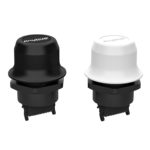
Once you settle on design specs, you’re ready to choose between a custom antenna design or a COTS antenna (Figure 2). Here, you have tradeoffs. For small quantities, you may choose a COTS antenna. Antenna manufacturers provide application notes that define the size of the ground plane you need. You’ll have strict requirements to meet to get optimum performance.
Figure 2. COTS antennas save you the pain of designing your own antenna, but they may not be cost effective in high volumes. Image: Ignion.
You also have mechanical constraints. “Do I have the space to use a COTS antenna, or will I need a custom design?” Product specs plus module performance influence the antenna design. You’ll have to account for TRP and TIS. The design spec plus the module performances help you define the antenna requirements. You may elect to work with virtual antennas, which bring the benefit of an easy design with the ability to simulate the end performance already from the start of the project and ensure meeting the TRP/TIS limits (using tools and services such as those available here). Custom antenna design requires specific expertise and simulation tools to achieve correct performances in the required form factor and to keep reasonable antenna cost.
Antenna characteristics over frequency include efficiency, return loss, gain, polarization (circular for GNSS, and vertical for cellular). The choice of COTS versus custom antenna often depends on manufacturing volume. Large quantities usually get a custom antenna design to match the enclosure. For shorter time to market in lower design cost, you may consider using a COTS antenna.
Hardware integration
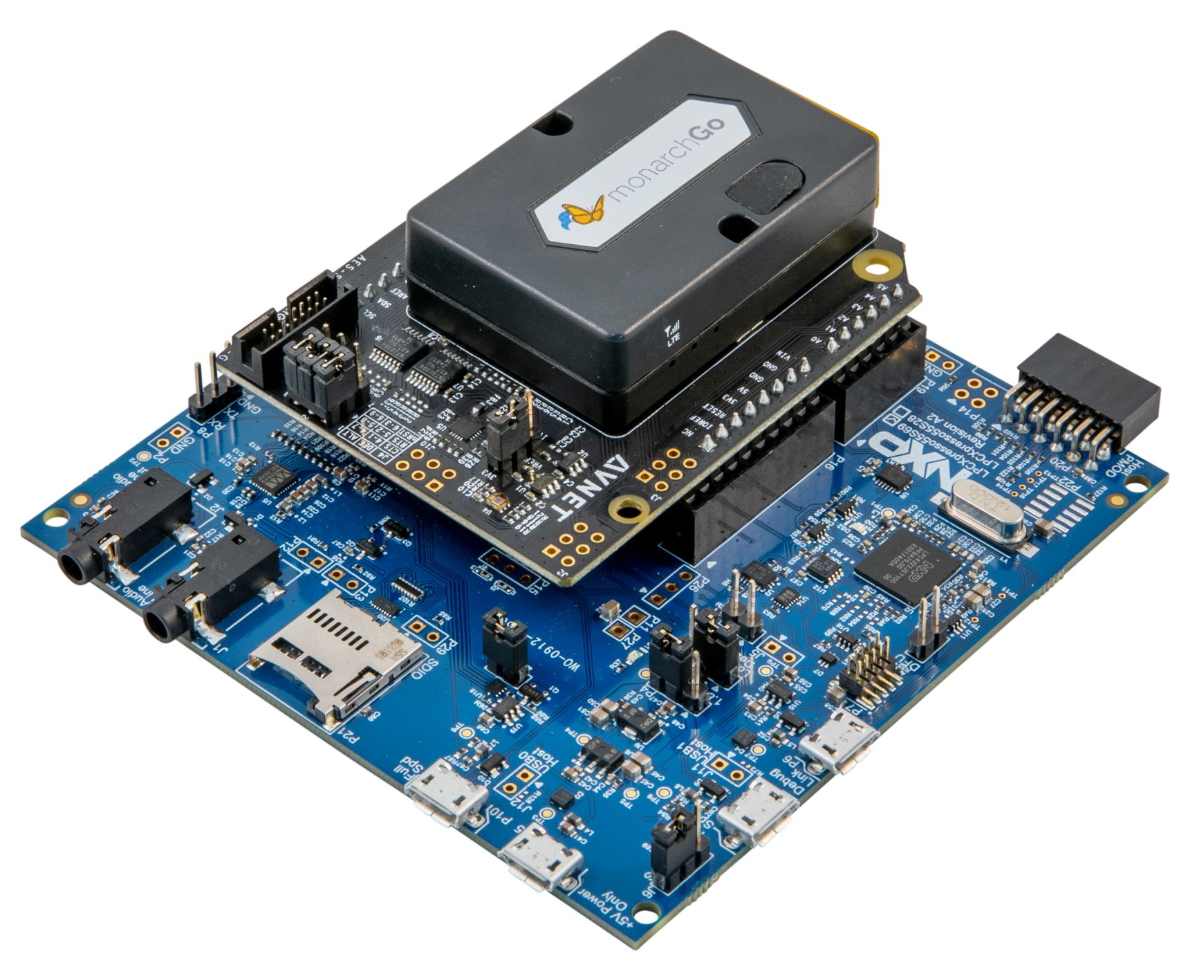
Figure 3. Design kits for wireless modules provide a platform for evaluating the device.
Module suppliers often provide design guidelines based on reference designs. Evaluation kits (Figure 3) contain the module, COTS antenna, antenna-tuning circuit, antenna matching, and RF connector on a board. Module manufacturers should provide design files, schematics, layouts, and characterization of the board’s performance. The kit lets you evaluate the performance of the module in a design. You should expect a development board to meet CTIA requirements for all the applicable bands.
While development kits make for a good start, they don’t emulate a user environment. That’s in part because development kits have more digital interfaces than you’ll use in your design. A typical development kit might include interfaces such as GPIO, UART, USB, SPI, JTAG, and so on. Your design may, for example, need to expose only two GPIOs and a UART. Getting optimal performance in the development kit is more complex than in most end applications – that’s one of the reasons why development kits are usually larger than final products.
When you use a digital interface, you add the risk of signal spurs and degradation that can reduce a receiver’s sensitivity. Module manufacturers can help by performing design reviews that include schematic and layout reviews with an eye towards RF performance. A careful design review will ensure that hardware integration of the module on the host PCB is optimal for both conducted and over-the-air (OTA) performance. Module vendors usually provide you with hardware design guidelines. Pay special attention to grounding, shielding, and isolation of any potential noise sources such as oscillators, high speed digital interface, DC/DC converters.
During the design preparation, you should anticipate manufacturing and qualification needs, by including test points, RF connectors for conducted testing, and adapting the antenna tuner to your product requirements.
Designs may also include other radios such as GPS, Wi-Fi, or Bluetooth. When such radios coexist, we recommend antenna isolation or digital mitigation. As an example, GPS receiver can coexist with other radios using GPS blanking feature, based on GPIOs, indicating when non-GPS transmission is taking place.
Although the module you choose must be certified to meet 3GPP requirements, you still must fully qualify and certify the final product. Industry and regulatory bodies will accredit the end device in its final form factor and will make sure that it is safe for operation on network.
From qualification to certification
Now that you have your hardware design ready and first prototypes available, next step is to qualify the RF performance. Indeed, how do you know if the overall design is good enough? What constraints do you have that might affect qualification? What is the recommended qualification flow that you must follow prior to bringing your product to certification?
During the hardware design cycle, the need of antenna matching, RF connector for conducted test, test points, antenna tuner have already been anticipated. Follow these steps in the qualification process.
- Ensure compliance to product specifications in conducted mode.
- Verify the antenna performances in passive mode.
- Verify the product performances (the combination of module, RF matching, tuner, and antenna) in active mode.
Coming back to step 1, you must verify key RF performances such as sensitivity, output power, and signal integrity. You can measure these key RF parameters with an LTE tester or go to a third-party lab. Module vendors can also propose such services to verify your design in conducted mode.
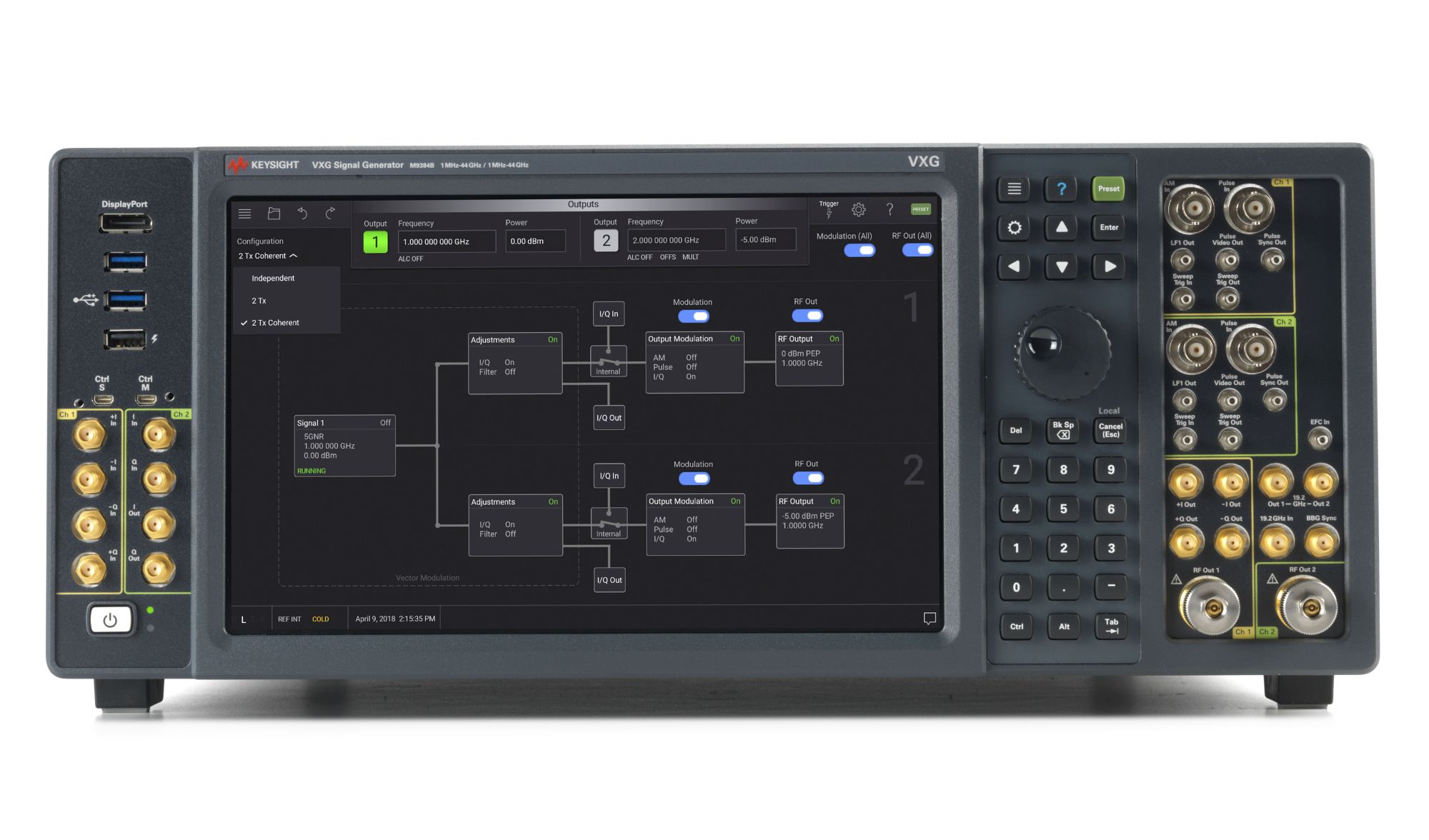
Figure 4. An RF signal generator let’s you perform passive tests on your prototype. Image: Keysight Technologies.
For step 2 you’ll need tests performed in a specialized over-the-air (OTA) chamber. Assume that you’re using a COTS antenna such as the one shown in Fig. 2. Some suppliers will offer services where you can send your prototype and they will perform a passive OTA test. We call these “passive measurements” because your product antenna is connected to a signal generator (Figure 4), placed inside an anechoic chamber, in which the intrinsic performance of the antenna will be measured (allowing antenna’s efficiency in all intended bands, return loss). That tells you if the antenna and tuning circuits are meeting requirements.
During the final qualification (step 3), you will test the module, RF matching, tuner, and integrated antenna, in active mode. That’s where you measure TIS and TRP. Mobile network operators are usually checking these two key criteria on final products and have strict requirements.
You should run these qualification tests at an early stage in the development so as to lock the hardware design. Keep in mind that conducted tests only get you so far. Assume you have DC-DC converter powering your MCU and module, and the converter radiates spurs in your targeted frequency range. If you don’t go through this qualification, you may not see the problem until you get to the certification lab. A late discovery will yield costly hardware redesign and will impact your ability to reach the market at the required timeline.
Even if your design passes certification requirements, a device with degraded RF performance draws excessive battery power. It may have poor performance in the field.
You must go through these steps to make sure that your product is certifiable and can be used on the googcommercial cellular network. If you’re developing a device such as a router that uses an external antenna where the enclosure can be shielded, then the risk is much lower than for a device with an internal antenna.
Once you’re ready with your hardware qualification, you must pass regulatory certification tests for individual regions, such as those for Japan (JATE, TELEC), or FCC in the U.S., RED in Europe, or UKCA in the UK. After that, your selected mobile network operator may ask you to perform dedicated product certification. At this stage, you have to perform, for example, TIS and TRP testing. Your operator may also ask you to confirm your compliance to industry certification standards, such as GCF or PTCRB.
Manufacturing test
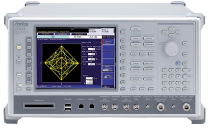
Figure 5. A spectrum analyzer or RF tester in manufacturing test lets you verify that a device is ready for the field. Image: Anritsu
While certification is important, don’t forget about manufacturing constraints.
There are usually three options to consider.
- No test during the end-device manufacturing: because the cellular module is tested before assembly, and when the manufacturing process is proven, the device manufacturer may consider that there is no need for final test in the manufacturing line. In such case, the final functional test is performed by the distributor or by the end customer, at first activation in the field.
- Test in non-signaling mode: this option involves a simple tester such as an RF signal generator, spectrum analyzer (Figure 5), or RF sensor . By doing this, the device manufacturer performs a sanity check, ensuring no major flaw in the full device assembly
- Test in signaling mode: this option involves an LTE callbox (an eNB emulator). By doing this, the device manufacturer performs a functional E2E test, mimicking what the device will face once in the field. Note that a test SIM card is used in such case.
Generally, for the latter two options, it’s mandatory to use a controlled RF OTA environment, such as a shielded box.