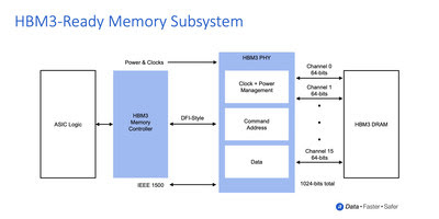
 Rambus Inc. announced the Rambus HBM3-ready memory interface subsystem consisting of a fully integrated PHY and digital controller. Supporting breakthrough data rates of up to 8.4 Gbps, the solution can deliver over a terabyte per second of bandwidth, more than double that of high-end HBM2E memory subsystems. With a market-leading position in HBM2/2E memory interface deployments, Rambus is ideally suited to enable customers’ implementations of accelerators using next-generation HBM3 memory.
Rambus achieves HBM3 operation of up to 8.4 Gbps leveraging over 30 years of high-speed signaling expertise, and a strong history of 2.5D memory system architecture design and enablement. In addition to the fully integrated HBM3-ready memory subsystem, Rambus provides its customers with interposer and package reference designs to speed their products to market.
Benefits of the Rambus HBM3-ready Memory Interface Subsystem: Supports up to 8.4 Gbps data rate delivering bandwidth of 1.075 Terabytes per second (TB/s); Reduces ASIC design complexity and speeds time to market with fully integrated PHY and digital controller; Delivers full bandwidth performance across all data traffic scenarios; Supports HBM3 RAS features; Includes built-in hardware-level performance activity monitor; Provides access to Rambus system and SI/PI experts helping ASIC designers to ensure maximum signal and power integrity for devices and systems; Includes 2.5D package and interposer reference design as part of IP license; Features LabStation development environment that enables quick system bring-up, characterization, and debug; Enables the highest performance in applications including state-of-the-art AI/ML training and high-performance computing (HPC) systems;