Gallium nitride (GaN) is a promising material for RF/mmWave and power applications because of its ability to operate at higher voltages and frequencies than silicon while exhibiting lower losses. The integration of GaN technology with CMOS technology, especially if built using mainstream silicon CMOS tools and fabrication processes, could usher in inexpensive next-generation PC/mobile devices that exhibit high performance and energy efficient operation. To this end, Intel researchers speaking at the upcoming 67th annual IEEE International Electron Devices Meeting--to be held Dec, 11–15, 2021 at the Hilton San Francisco Union Square hotel–will describe a highly scaled, high-performance, enhancement-mode high-k GaN-on-Si NMOS FinFET built on a 300-mm Si platform and integrated with Si PMOS FinFET technology.
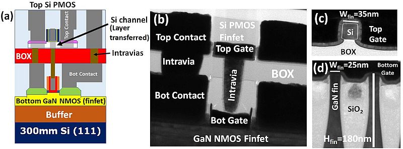
(b) the fabricated 3D layer-transfer stacked inverter, comprising a bottom GaN E-mode high-k NMOS FinFET transistor and a top Si PMOS FinFET transistor
(c) a 35-nm-wide Si fin as the top PMOS channel
(d) a 25-nm-wide GaN fin as the bottom NMOS channel – this is the narrowest GaN fin with the highest aspect ratio (Hfin/Wfin=7) ever demonstrated in literature. The narrow transistor widths of the FinFET architecture enable low leakage currents in logic applications. Click image to enlarge.
The heterogeneous device was made possible by a layer-transfer technique Intel first described at the 2019 IEEE IEDM that enables GaN NMOS and Si PMOS devices to be fabricated in parallel. The NMOS GaN FinFET features the narrowest GaN fin to date (width=25 nm); an ultra-short gate length (30 nm); and is integrated with a Si PMOS FinFET having a fin width=35 nm. The device represents many industry firsts and records for GaN-on-Si, including a record fT/fMAX of 300/400 GHz and record transconductance (GM>2.100 µS/µm) with the industry’s thinnest TOXE (14.8Å), among others. It is the first true enhancement-mode (i.e., “normally off”) GaN transistor with IOFF <25 pA/µm (up to VD=30 V).
The researchers demonstrated the technology by building a low-loss inverter with it. They say that going forward, GaN FinFET architectures and 3D layer-transfer technologies will play a significant role in GaN device scaling and in the ability to integrate more functionalities like CMOS with GaN technology. (Paper #11.1, “Advanced Scaling of Enhancement-Mode High-K Gallium Nitride-on-300mm-Si(111) Transistor and 3D Layer Transfer GaN-Silicon FinFET CMOS Integration,” H.W. Then et al, Intel)
At the IEEE IEDM each year, the world’s best scientists and engineers in the field gather to participate in a technical program consisting of more than 220 presentations, along with a variety of panels, Focus Sessions, Tutorials, Short Courses, IEEE/EDS award presentations, a supplier exhibit and other events which highlight leading work in more areas of the field than any other conference.
Here are details of the 2021 IEEE IEDM:
90-Minute Tutorials – Saturday, Dec. 11
The 90-minute Saturday tutorial sessions on emerging technologies have become a popular and growing part of the IEEE IEDM. They are presented by experts in the field to bridge the gap between textbook-level knowledge and leading-edge current research, and to introduce attendees to new fields of interest:
2:45 p.m. – 4:15 p.m.
Beyond the FinFET Era: Challenges and Opportunities for CMOS Technology, Kai Zhao, IBM
TCAD-Based DTCO and STCO, Asen Asenov, University of Glasgow
6G Technology Challenges from Devices to Wireless Systems, Aarno Pärssinen, Oulu University
4:30 p.m. – 6:00 p.m.
Selective and Atomic-Scale Processes for Advanced Semiconductor Manufacturing, Robert Clark, TEL
Machine Learning for Semiconductor Device and Circuit Modeling, Elyse Rosenbaum, University of Illinois, Urbana-Champaign
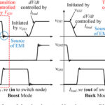
GaN Power Device Technology and Reliability, Dong Seup Lee, Texas Instruments
IEDM Short Courses – Sunday, Dec. 12
In contrast to the Tutorials, the full-day Short Courses are focused on a single technical topic. Early registration is recommended, as they are often sold out. They offer the opportunity to learn about important areas and developments, and to network with global experts.
Future Scaling and Integration Technology, organized by Dechao Guo, IBM Research
Processes and Materials Engineering Innovations for Advanced Logic Transistor Scaling, Benjamin Colombeau, Applied Materials
Interconnect Resistivity: New Materials, Daniel Gall, Rensselaer Polytechnic Institute
Metrology and Material Characterization for the Era of 3D Logic and Memory, Roy Koret, Nova Ltd.
Beyond FinFET Devices: GAA, CFET, 2D Material FET, Chung-Hsun Lin, Intel
Heterogenous Integration Using Chiplets & Advanced Packaging, Madhavan Swaminathan, Georgia Tech
Design-Technology Co-Optimization/System-Technology Co-Optimization, Victor Moroz, Synopsys
Emerging Technologies for Low-Power Edge Computing, organized by Huaqiang Wu, Tsinghua University and John Paul Strachan, Forschungszentrum Jülich
Mobile NPUs for Intelligent Human/Computer Interaction, Hoi-Jun Yoo, KAIST
Brain-Inspired Strategies for Optimizing the Design of Neuromorphic Sensory-Processing Systems, Giacomo Indiveri, University of Zurich
Memory-Based AI & Data Analytics Solutions, Euicheol Lim, SK hynix
Material Strategies for Memristor-Based AI Hardware and their Heterointegration, Jeehwan Kim, MIT
RRAM Devices for Data Storage and In-Memory Computing, Wei Lu, University of Michigan
Practical Implementation of Wireless Power Transfer, Hubregt Visser, IMEC
Plenary Presentations – Monday, Dec. 13
The Smallest Engine Transforming Our Future: Our Journey Into Eternity Has Only Begun, Kinam Kim, Vice Chairman & CEO, Samsung Electronics Device Solutions Division
Creating the Future: Augmented Reality, the Next Human-Machine Interface, Michael Abrash, Chief Scientist, Facebook Reality Labs
Quantum Computing Technology, Heike Riel, Head of Science & Technology, IBM Research and IBM Fellow
Luncheon – Tuesday, Dec. 14
There will be a career-focused luncheon featuring industry and scientific leaders talking about their personal experiences in the context of career growth. The speakers will be:
Sophie Vandebroek, Founder & Owner, Strategic Vision Ventures LLC. Dr. Vandebroek is a seasoned executive with extensive C-level experience at IBM, Xerox and UTC, and has served on public and private company boards since 2008. She is an expert in the creation and application of technologies that drive growth, and in the governance of inclusive and innovative global organizations. Dr. Vandebroek was previously VP of Emerging Technology Partnerships for IBM; Chief Operating Officer of IBM Research; CTO and Corporate Vice President at Xerox; and Board Chair of Xerox PARC, among other noteworthy roles.
Deji Akinwande, Temple Foundation Endowed Professor at the University of Texas at Austin. Dr. Akinwande invented 2D memory, also known as atomristors. He has been honored with the 2018 Fulbright Specialist Award, 2017 Bessel-Humboldt Research Award, the U.S Presidential PECASE award by President Obama, the inaugural Gordon Moore Inventor Fellow award, the inaugural IEEE Nano Geim and Novoselov Graphene Prize, the IEEE “Early Career Award” in Nanotechnology, the NSF CAREER award, and several DoD Young Investigator awards, among many others.
Evening Panel Session – Tuesday evening, Dec. 14
A staple of the IEEE IEDM conference is the evening panel session, an interactive forum where experts give their views on important industry topics, and audience participation is encouraged to foster an open and vigorous exchange of ideas. The title of this year’s evening panel is “Is Hardware/Software Co-Design a Necessary Evil or a Symbiotic Partnership?” Moderated by Myung-hee Na, Semiconductor Technologist and VP of the Revolutionary Technology Center at SK hynix, it will explore the idea of what hardware/software co-design really means in terms of technology development and the introduction of new technology.
Further information about IEDM
For registration and other information, visit www.ieee-iedm.org.