Modern analog/digital converters can help implement equivalent time sampling to provide picosecond timing resolution.
Dave Guidry, Texas Instruments Inc.
A picosecond is an astonishingly short period of time. Imagine a stopwatch with a trillion divisions between each tick of the second hand. While it sounds fantastical, this resolution of time measurement is indeed necessary for a diverse set of applications, including quantum computing, particle physics, automatic test equipment (ATE) and phased-array radars.
Measurement of time on this scale has traditionally been a quite complex and expensive endeavor requiring specialized instrumentation. Now, features in modern analog-to-digital converters (ADCs) make picosecond-resolution time measurement possible without breaking the bank.
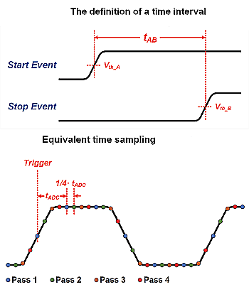
Time measurement is often defined as the difference in time between a start and a stop event. In modern electronics, the time interval will likely be between two high-speed digital signals where the event is the moment when the signal transitions through a predefined threshold.
Instruments that can precisely measure the time difference between two events are known as time interval counters or time measurement units. These can be quite complex and expensive instruments, especially when picosecond resolutions are required.
A generic time interval measurement does not assume a relationship between the start event or stop event. Thus, the instrument must fully resolve the time difference between two asynchronous events. There is no easy way to accomplish this task with discrete circuitry; only specialized – and likely expensive – hardware will work.
Many time-interval measurement applications do, however, involve measuring the difference between events that have a known relationship. For instance, the skew between two outputs of a clock distribution network will not only have the same frequency as each other, but also the same frequency as the input signal. Leveraging this fact enables the use of equivalent time sampling.
Equivalent time sampling explained
Sampling theory specifies the need for at least two samples per period of the highest frequency signal measured. This reality, defined by Nyquist, is impossible to avoid, but you can sidestep it if the input signal measured is repetitive.
Consider an example involving an ADC. The above figure shows a fourfold increase in the effective sample rate from that of the ADC sample rate. Each triggered measurement captures six samples per cycle of the input waveform. Between triggers, I delayed the sampling clock for the ADC by one-fourth the sample period. I then took the four sets of six samples and interleaved them to produce a resulting waveform that boosted the sample rate fourfold. This scheme is widely used in digital storage oscilloscopes to increase the effective sample rate for repetitive signal measurement and can achieve sample rates of hundreds or even thousands of gigasamples per second.
An alternate to equivalent time sampling is known as coherent undersampling. Instead of using an analog delay to adjust the sampling instant between each triggered capture, undersampling changes the sample rate slightly to create a beat frequency between the input frequency and the clock frequency. This technique has the same effect as equivalent time sampling (in other words, each input period slips a small amount of time), but does not require an adjustable analog delay. The downside to this approach is that it requires a synthesizer with a high-frequency resolution to create the sample clock frequency.
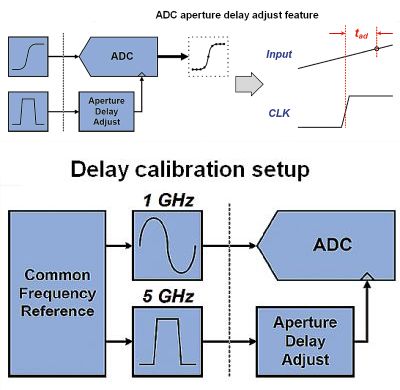
Fortunately, features of Texas Instruments high-speed ADCs can help implement equivalent time sampling without any special clock synthesizer or external adjustable analog delay components. TI has released three high-speed ADC families that employ a feature known as aperture delay adjust. Before diving into how this feature can provide picosecond resolution, a brief introduction is in order.
Aperture delay is the time from when the clock transitions until the ADC sample-and-hold captures the input signal. Every ADC experiences aperture delay because its circuitry has a finite propagation delay, but the TI family of high-speed ADCs add a feature to make aperture delay adjustable, with an astounding 19-fsec resolution. A femtosecond is 1/1,000th of a picosecond, or a quadrillionth of a second.
The aperture delay-adjust feature is implemented in such a way that it is largely unaffected by temperature, process or supply-voltage variations, and has minimal impact on sampling jitter. This quality is especially useful for time interval measurements because there is a high-resolution delay feature that can be used to implement equivalent time sampling.
These ADCs have an inherent typical aperture delay of 360 psec, with the aperture delay adjust feature set at its minimum. Up to about 600 psec of additional aperture delay can be added by setting 8-bit coarse and fine settings, with 1.13-psec and 19-fsec step sizes, respectively. For sample rates below about 1.67 GS/sec, the sample clock can be inverted to boost the delay range by half of the sample clock period. This means that any sample rate over about 833 MSPS will have full coverage across the sample period to adjust the sampling point.
Calibrating delay
Though it is stable, the aperture delay-adjust feature is not factory-calibrated. But one can easily employ a calibration routine to select the optimal coarse and fine aperture delay settings for each desired delay value. For example, operating the ADC12DJ5200RF in dual-channel mode at 5 GSPS results in a 200-psec sample period, which the aperture delay-adjust feature then further subdivides into 1-psec time slices, yielding an effective sample rate of 1,000 GS/sec.
The most straightforward way to calibrate the delay settings is to use a fixed coherent input frequency with respect to the sample clock where you can measure changes in phase (and thus time) across aperture delay settings. The input need not be high fidelity as long as it is phase-stable, an integer frequency ratio, and sufficiently low-jitter with respect to the sample clock. I selected 1-GHz for the purposes of this article, which results in five samples per period of the 5-GS/sec clock.
The nearby figure illustrates the setup for calibration. I adjusted the input signal amplitude to -1 dBFS to optimize the signal-to-noise ratio – but that adjustment is not a strict requirement. I captured 50,000 samples for each measurement, then divided the measurements into 10,000 arrays of five samples each. Averaging these arrays sample by sample resulted in a five-sample array.
This five-sample array represents one cycle of the calibration signal averaged 10,000 times. Taking the unwindowed Fast Fourier transform of this array results in an optimal estimation of the phase of the signal. If you trigger subsequent captures to start at the same place, multiple captures can then be further averaged to mitigate the impact of low-frequency noise (also known as 1/f noise).
Remember: You are calibrating the differential delay between what is defined as the “zero” delay setting and each relative delay setting. The absolute delay over any significant period of time will drift because of temperature changes in the interconnect cables, clock and input-signal generators. While these changes may be seem small, without mitigation, the calibration will skew by as much as several picoseconds.
The solution to this problem is thankfully straightforward. For each delay setting, simply measure the
delta delay between the zero-delay setting and the coarse and fine settings under inspection. Repeating this measurement a sufficient number of times will mitigate low-frequency noise until you’ve attained the desired precision.
Again, the coarse and fine delays have approximately 1.13-psec and 19-fsec step sizes, respectively. If you are searching for 1-psec steps, a number of possible combinations of coarse and fine delay will result in several delay values close to your target. This procedure helps realize a convergent calibration, as there are multiple ways to get to each 1-psec step.
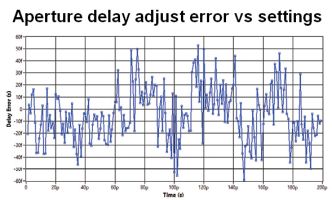
The nearby figure shows the resulting residual error for each 1-psec delay setting after calibration. At less than ±60 fsec, it is difficult to appreciate the small size of this error. In a vacuum, light travels a mere 18 µm in 60 fsec–and perhaps only 60% to 70% of this distance–in a typical high-speed circuit board.
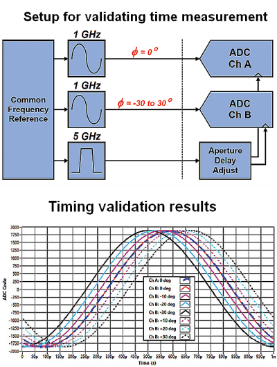
In the setup used to validate the calibration of the delay settings, each channel of the ADC is driven with an independent 1-GHz signal generator. Both signal generators are locked to the same common frequency reference as the ADC clock generator. This phase locking ensures phase stability between the ADC inputs and enables the use of coherent sampling. The synchronization of captures to the input frequency ensures that the recovered waveform has the same phase each time.
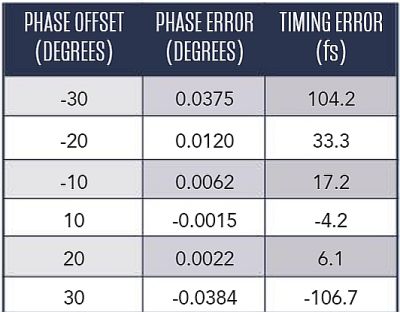
Before collecting data, I adjusted the phase and amplitude of the generator driving channel B to minimize the difference between the channels. I used a Rohde & Schwarz SGS100A 12-GHz RF generator, which has a phase offset capability with 0.1° resolution. With this adjustment, it was possible to get both signals aligned within about 0.5 psec.
I set the channel B signal generator to a phase offset of -30 to +30° in 10° steps. At each offset, I captured and compared the signal to the phase of channel A, which was left at its initial setting.
A practical example
To relate the practical reality of tightly aligning clock signals in a distribution network, I employed the output of a LMK04832 clock dual-loop jitter cleaner and clock distribution IC to convert the sine wave from the RF signal generator into a low-voltage positive emitter-coupled-logic square wave. I used an RF power divider to split this signal into two copies, which were then connected to both ADC channels using six-inch phase-matched cables.
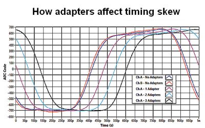
The “well-matched” distribution path has about 9 psec of skew, which is attributable to the combination of mismatch in the cables, splitter, PCB interconnect and ADC itself. Adding a subminiature version A (SMA) “connector saver” adapter, which seems innocuous, causes an increase in skew of 62 psec to 6 psec per adapter. This figure is quite close to what you’d expect for an addition of about a half-inch-worth of transmission line with a PTFE dielectric.
This skew further enforces the difficulty in trying to tightly match timing across high-speed systems and the need for a high-resolution instrument to measure skew. In the example, it’s clear that a simple RF adapter may be enough to consume a significant portion of the timing budget.
All in all, equivalent time sampling is a simple and cost-effective way to realize high-resolution time measurement of repetitive signals. The aperture-adjust feature in TI’s family of high-speed ADCs enables 1-psec time resolution and precision in the order of ±100 fsec. The ADC12DL3200, ADC12DJ3200 and ADC12DJ5200RF families all incorporate this aperture-adjust feature.