The first two FAQs in this series considered the potential for metamaterials to have significant impacts on advanced optics, audio systems, thermal management, and various aspects of mmWave communications and radar. This final FAQ will consider the impact metamaterials are expected to have on energy harvesting (both solar electric and solar thermal) high-power long-distance power transmissions and wireless charging. Several of these are early commercial-stage technologies undergoing field trials.
Development of metamaterials is a complex process. The name is derived from the Greek word “meta” meaning “beyond” and the Latin “materia” meaning “matter” or “material.” The field is multi-disciplinary and includes electrical engineering, semiconductors, electromagnetics, microwave and antenna engineering, optoelectronics, classical optics, solid state physics, material sciences and nanoengineering.
The properties of metamaterials are not based on the properties of the base materials, they are based on engineering the physical structure of a composite material. Metamaterials are fashioned from assemblies of multiple elements consisting of composite materials such as metals, plastics, ceramics, and so on. Metamaterials rely on precises geometry/shape, size, orientation and arrangement to derive their properties that extend beyond what is possible with naturally occurring materials.
Energy harvesting
A patented metamaterial-based coating has been developed that looks opaque but is substantially transmissive of light. It can be applied over solar cells to conceal them, while they continue to generate electricity. The coating is composed of microspheres with diameters under 5 microns that have 30 or more layers of materials with varying dielectric properties. Engineering the correct materials for the various layers results selective scattering of specific wavelengths of light, producing a controlled color appearance on the surface, while still being transparent to the majority of impinging light wavelengths.
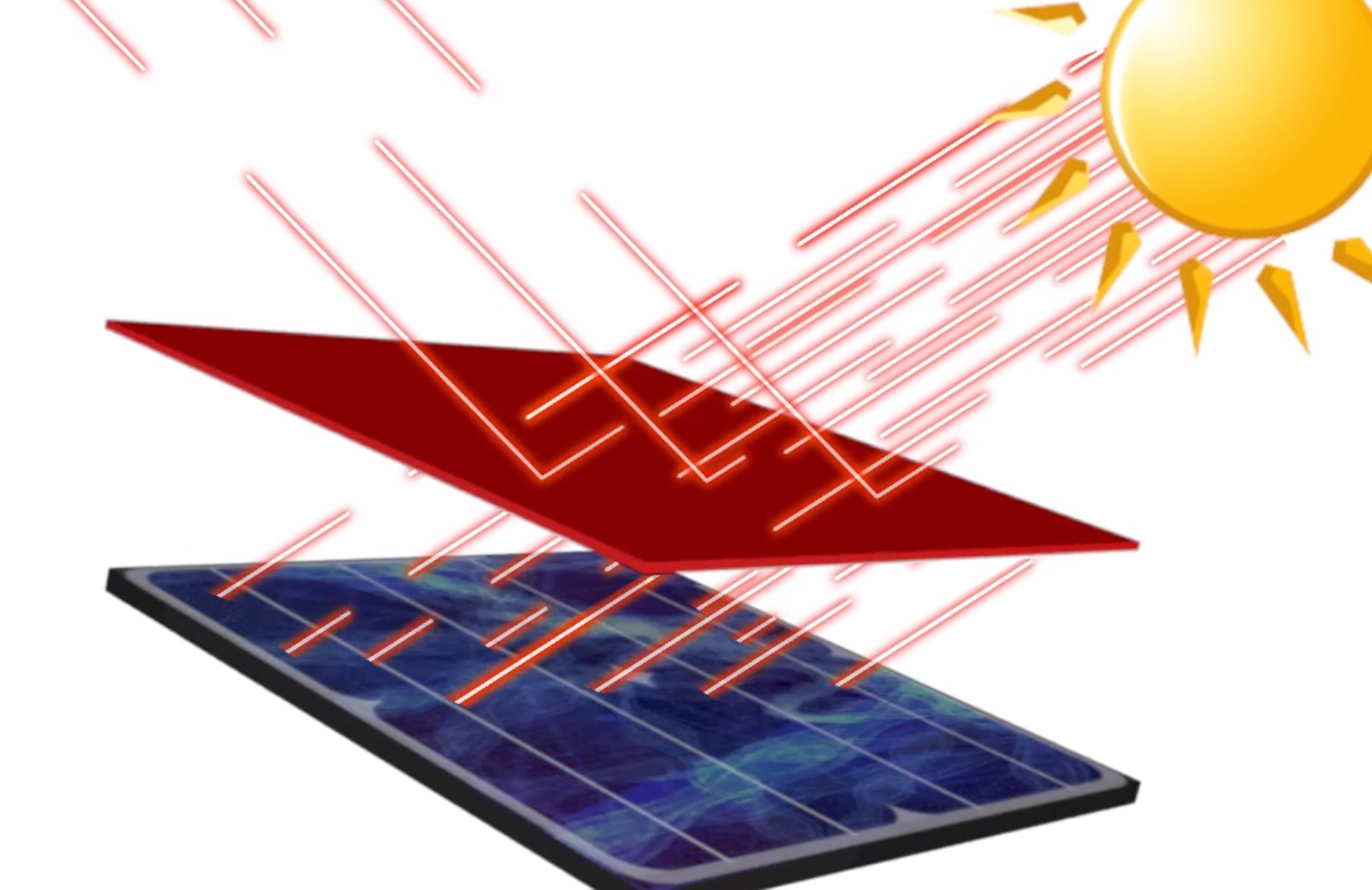
The binding used to apply the microspheres can be solvent- or water-based. The color of the coating is solely dependent on the structure of the microspheres, so it does not fade over time. In conventional paints, the chemical-based pigment degrades and the color fades over time. The durability of the metamaterial coating is similar to that of high-performance paints such as automotive finishes. And it can be applied withthe same processes used to apply conventional paints. Anticipated applications for this new metamaterial coating include:
- Solar roofing and building components that harvest solar energy, but appear just like their conventional non-energy harvesting counterparts
- Solar harvesting systems that blend seamlessly into natural settings, remote locations, wilderness, etc., with no ugly solar cell arrays visible
- Covert surveillance devices that can look like almost any object
- Solar and light harvesting body panels for electric vehicles without sacrificing aesthetics
In addition to the metamaterials being developed for thermal management (discussed in the first FAQ in this series, “Metamaterials’ potential for transforming electronics”), metamaterials are being developed to implement thermal energy harvesting. For example, a solar-thermal absorber should have selective absorption, high thermal conductivity, stability over time and a simple structure. A three-dimensional structured graphene metamaterial (SGM) is being explored by a group of Australian researchers. SGM exhibits wavelength selectivity as a result of its trench-link metallic structure, broadband capabilities and excellent thermal conductivity.
As an ultrathin graphene metamaterial, SGM absorbers have been demonstrated with selective and omnidirectional solar absorption, and excellent photothermal capabilities. They are very stable and have exhibited solar-to-thermal conversion efficiency of 90.1% and solar-to-vapor efficiency of 96.2% efforts are currently underway to develop commercial devices based on SGM absorbers for use in solar thermal energy harvesting and manipulation.
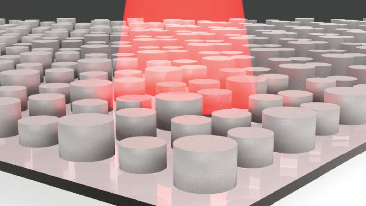
Another group of electrical engineers has harnessed the power of machine learning to design dielectric (non-metal) metamaterials that absorb and emit specific frequencies of terahertz radiation. In this case, the terahertz metamaterial is built up from a two-by-two grid of silicon cylinders. Adjusting the height, radius and spacing of each of the four cylinders changes the frequencies of light the metamaterial interacts with. These thermophotovoltaic devices generate electricity from heat sources. They work much like solar panels, except they absorb specific frequencies of infrared light instead of visible light.
Power transmission
New Zealand-based start-up Emrod has developed what is thought to be the world’s first long-range, high-wattage, wireless power transmission system as an alternative to existing wire line technology. The Emrod technology works by utilizing electromagnetic waves to safely and efficiently transmit energy wirelessly over long distances. A proof-of-concept prototype has been built and the company is now working with Powerco, New Zealand’s second-largest power distributor, to conduct a commercial-scale trial of the technology.
A combination of beam shaping, metamaterials and rectenna technologies is used to create columnated energy beams that can transmit large amounts of power over many kilometers. The system is not affected by weather, or atmospheric conditions such as rain, fog or dust. A low-power laser safety curtain around the power beam shuts down the system before any object (ranging from birds to helicopters) can impinge on the beam, the system restarts once the interfering object leaves the beam area. Advantages claimed for this metamaterials-enabled wireless power transmission technology include:
- Up to 65% reduction in electricity infrastructure costs.
- Up to 85% reduction in outages.
- Increases potential for sustainable energy use by reducing infrastructure costs.
- Fewer failure points compared with conventional copper-base power transmission, increasing system reliability.
- Uses beams in the ISM (industrial, scientific, medical) band with frequencies commonly used in WiFi, Bluetooth and RFID.
- Safer than conventional power transmission, with reduced risks of electrocution.
Wireless charging
In addition to transmitting high wattages over long distances, metamaterials hold the promise for substantially improving the efficiency of lower-power wireless charging systems. Power transfer efficiency can be improved significantly with negative-index metamaterials (NIMs). NIMs are characterized by a negative index of refraction. No naturally-occurring materials have been identified that exhibit a negative index of refraction.
With a flat slab of NIM, negative refraction can happen at both interfaces. When an object is in front of such a slab, the propagating wave components of the object can be focused inside the NIM slab, and refocused on the other side of the slab. Moreover, evanescent wave components can be enhanced inside a NIM slab to levels similar to the levels adjacent to the original electrical conductor. Similarly, with a NIM slab, evanescent waves of an object can be restored at a distance far greater than the classical distance of λ/3. This means, a NIM slab recovers both propagating waves and evanescent waves of an object and makes a “perfect lens.”
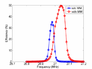
Researchers at Mitsubishi Electric Research Laboratories have built a prototype wireless power transfer system incorporating a NIM lens. Experiment results (see image above) prove the efficiency improvement with the fabricated metamaterial. The system with metamaterial is capable of transferring power wirelessly at roughly double the efficiency of the same system without a metamaterial. One potential application for NIM lenses is in charging electric vehicles. The NIM lens would be part of the vehicle’s power receiver sub system and would drop from the bottom of the vehicle and be stationed between the receiver and sender coils to improve charging efficiencies.
That concludes this FAQ series on metamaterials. The series has included both current commercial examples and research and development activities related to metamaterials. You may also be interested in reading part one, “Metamaterials’ potential for transforming electronics” and part two, “Metamaterials, mmWave antennas, 3D radar and holographic beamforming.”
References
Machine Learning Finds New Metamaterial Designs for Energy Harvesting, Duke University
Metamaterial, Wikipedia
Structured graphene metamaterial selective absorbers for high efficiency and omnidirectional solar thermal energy conversion, Nature Communications
Wireless power transfer with metamaterials, Researchgate