Measuring and determining 1/f voltage noise over a multiple-year sample requires an operational amplifier and effective 1/f knowledge. This article shows how to identify and determine the actual op amp 1/f voltage noise across a sample size of years and explains why the 1/f voltage noise is a non-issue at higher frequencies.
After many years of using operational amplifiers (op-amps), it is still a mystery that the exceedingly high voltage values of 1/f noise present no worries for my designs. But I hate mysteries. This prompts me to look at the 1/f phenomenon a little closer.
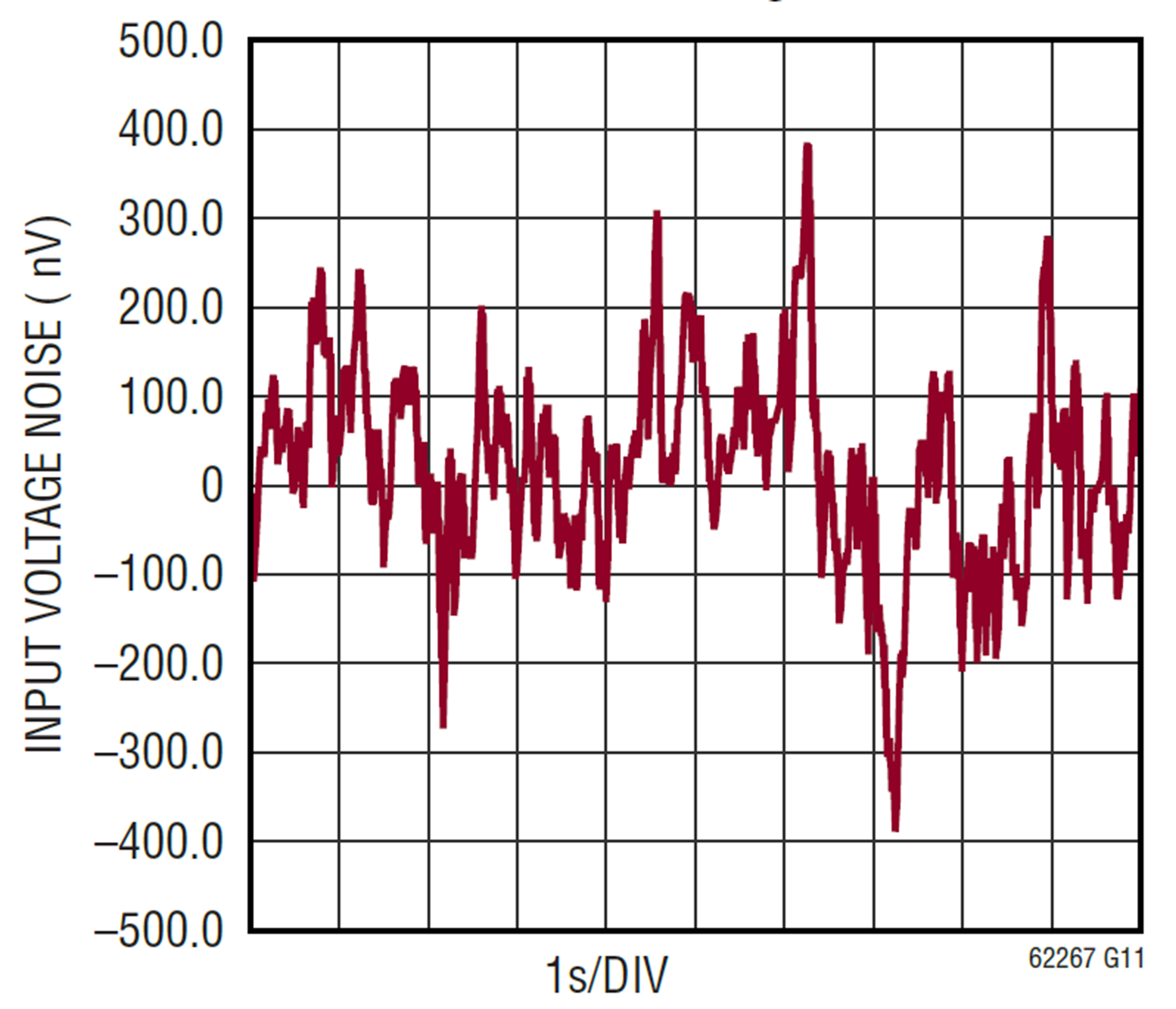
Pink noise, flicker, or the 1/f noise spectrum is inversely proportional to frequency. This noise appears to flutter or move irregularly or unsteadily like shadows flickering from a candle in the window (Figure 1).
Equation 1 exhibits an approximation of 1/f spot noise.
 Where X(f) is voltage or current
f is frequency in Hertz
is constant between 0 and 2, but more likely close to 1
You can find 1/f noise in all active electronic devices as well as some passive devices. In electronics, 1/f voltage noise is a byproduct of impurities in a conductive channel or transistor base current generation and recombination. Of the three resistor types (wire wound, film type, and composition), the composition resistor exhibits 1/f contact noise as a result of the individual particles molded together. For composition resistors, 1/f noise is current dependent as voltage noise increases with increasing current.
With op-amps and voltage references, the datasheet 0.1Hz to 10Hz frequencies is the 1/f noise specification range. Additionally, most op-amps have noise plots that include the 1/f noise performance range. I will explain the significance of the op-amp noise plot and talk about the long-term noise measurements in standard amplifiers.
Standard op-amp voltage noise
Most op-amps have two areas where the noise specifications are available. The first area is in the electrical characteristic table. Under the noise category, there is a referred-to-input (RTI) peak-to-peak voltage noise, RTI voltage noise density, and RTI current noise density.
The peak-to-peak input voltage noise captures the 1/f data with microvolts peak-to-peak (mVpp) units, typically a frequency range of 0.1Hz to 10Hz. The derivation of the peak-to-peak from the datasheet values equals the RMS value times six. Root-mean-sum (RMS) noise is the graphical, mathematical area under the noise curve across a specified frequency range. Also, keep in mind that the 1/f period for a 0.1Hz to 10Hz is 10 seconds.
A second specification is the noise density, which captures the op-amps broadband input noise at specific frequencies. A specified standard frequency may be 1kHz to 10kHz, and the typical input voltage noise unit is nano-volts per root hertz (nV/√Hz).
An additional area with the op-amp noise characteristics is in the typical characteristic curves. One can see graphically what the 1/f and broadband noise looks like (Figure 2).
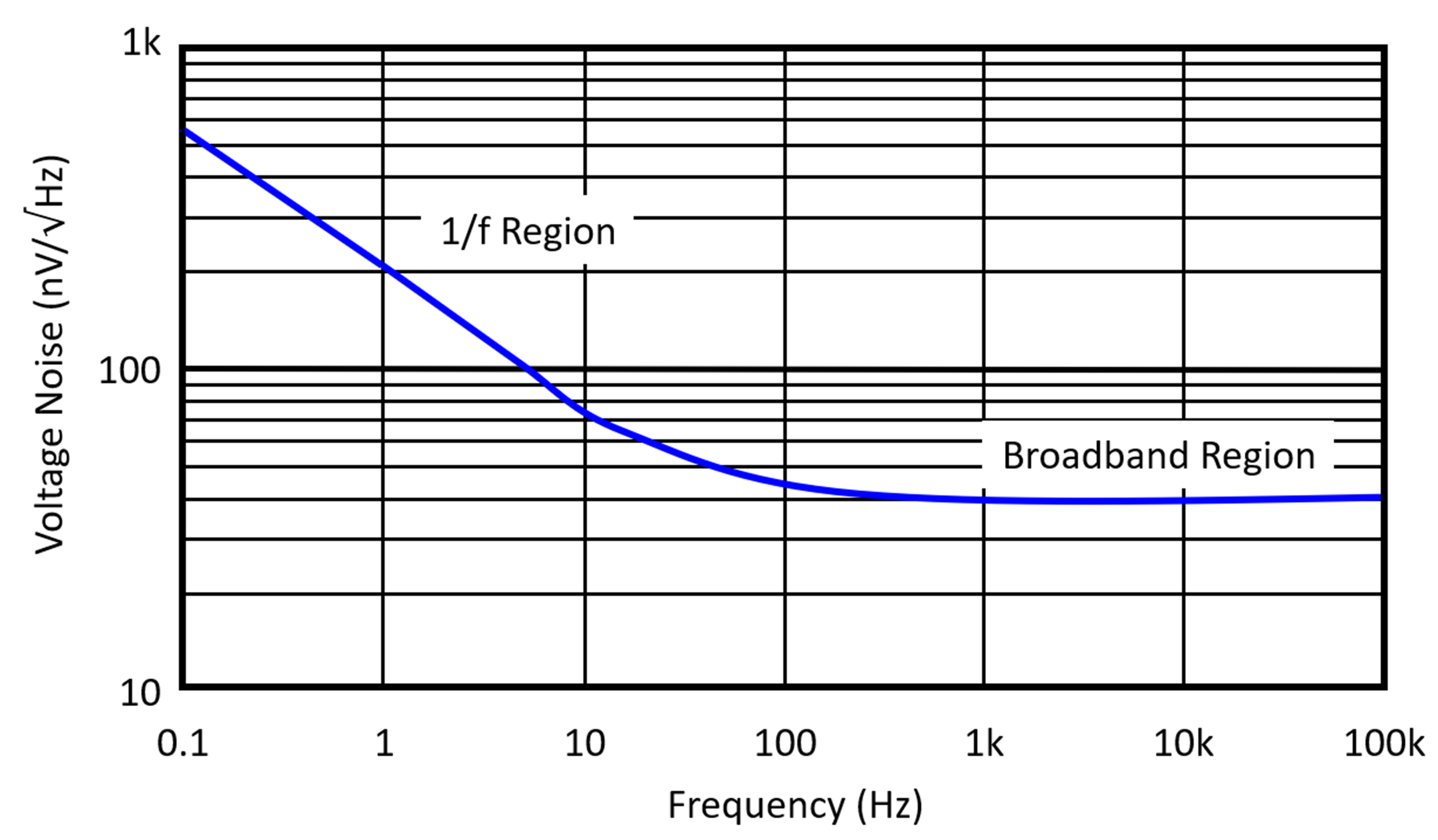
In Figure 2, the Texas Instruments’ OPA336 1/f noise region attenuates with increased frequency. The corner frequency between the 1/f and broadband region curves is ~100Hz. If you extrapolate before this curve with decreasing frequency, the voltage noise magnitude continues to climb. It also appears that the area under 0.1Hz to 1Hz is considerably more significant than the area under the 1Hz to 10Hz region, but it is not. Keep in mind, the area formula includes linear noise times the logarithmic frequency, where the frequency values have a considerable impact on the results. The area, and hence noise value, between 1Hz and 10Hz, is equivalent to the area between 0.1Hz and 1Hz.
Noise for all 1/f decades
Each frequency octave in the 1/f region has an equal amount of RMS or peak-to-peak voltage noise, prompting an investigation into looking at noise in longer time intervals.
The inverse of 0.1Hz equals ten seconds. With respect to electronics, this may seem like a long time, but some applications require even more time. The question is, what is the 1/f noise for days, months, or years?
Equation 2 shows the 1/f noise calculation across varying frequencies.
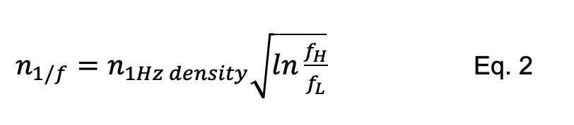
Where n1/f units are Volts RMS
n1Hz density is the value of the device’s noise at 1 Hz (units is volts/√Hz)
fH is the higher frequency from the range
fL is the lower frequency from the range
For instance, if the noise density of a device at 1Hz equals 200nV and the range under consideration is from 1Hz to 10Hz, the generated peak-to-peak noise equals:
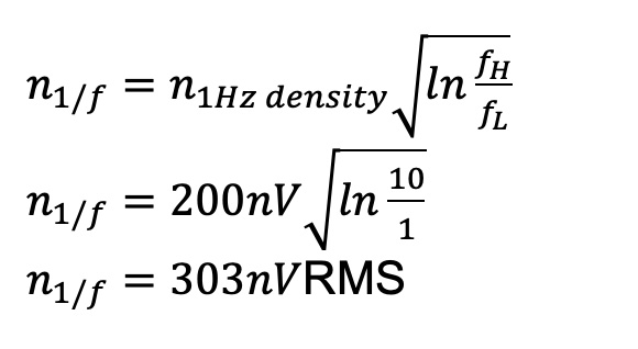
For the range of the 1/f volts RMS noise from 1Hz (1 second) to 10Hz (0.1 seconds), the peak-to-peak value of 303mVRMS equals 1.818mVp-p. Table 1 shows how this calculation applies to various frequency and time ranges.
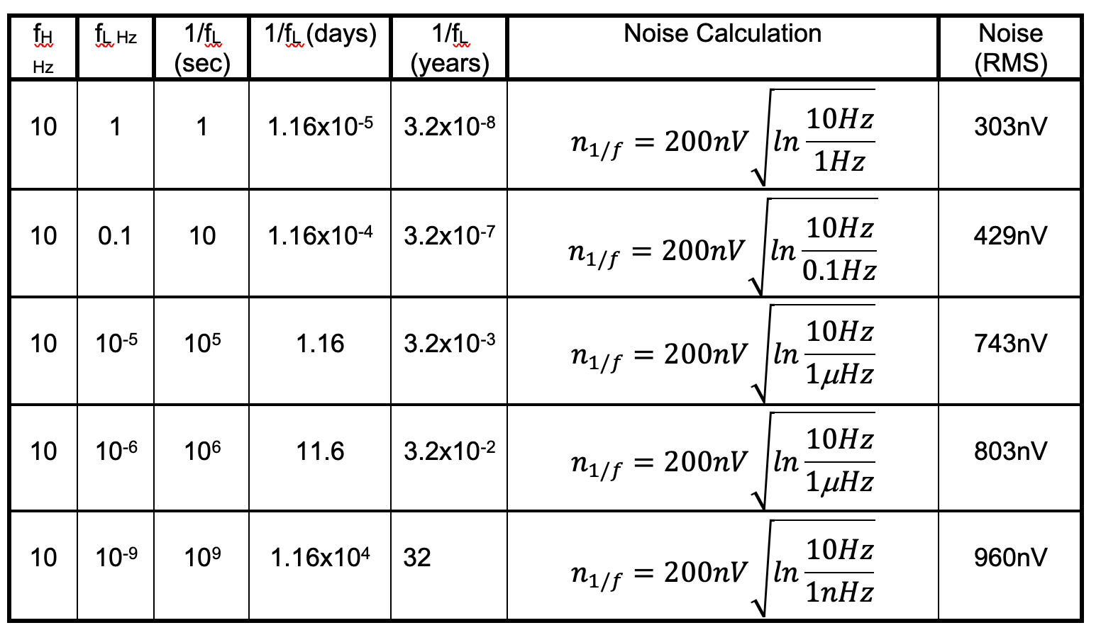
This table shows how 1/f noise occurs over long-time intervals. It is useful to observe that the calculation uses the high and low-frequency ratio, so as Figure 2 indicates the total noise between 1Hz and 10Hz is equivalent to the noise between 0.1Hz and 1Hz.
1/f in the time domain
Now let’s go back to the beginning of the article and look at 1/f in the time domain. Figure 3 shows the OPA336 op-amp’s time domain noise from two different time perspectives. As expected, the peak-to-peak noise increases for longer periods.
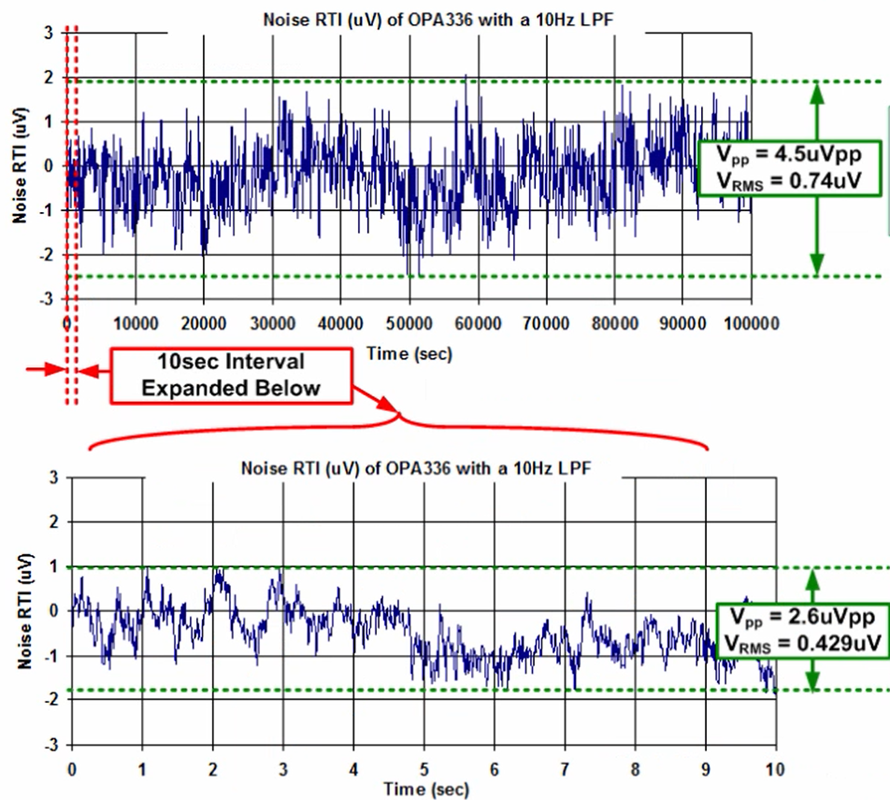
The top waveform shows 100,000 samples of the OPA336 noise over approximately 1.2 days. As expected, over this time, the peak-to-peak span seems to be higher than the bottom waveform at 4.5mVpp and 0.74mVRMS, which matches the calculations in Table 1. If you snatch any 10-second subinterval from the top graph, the total RMS noise consistently reduces, as the calculation shows.
In this example, a 10-second subinterval shows a total noise of 0.43 microvolts RMS. The first 10 seconds of the top graph have approximately the same total RMS noise. Remember that a smaller period corresponds to a more significant, lower cut frequency, and therefore, less area under the 1/f curve.
We can take an extrapolation of the concept to higher frequencies. A bandwidth 10kHz to 100kHz is an appropriate sampling range for many instrumentation applications. The area under the noise curve from 10KHz to 100kHz is equal to:
nRMS = 4nV * (100kHz-10kHz)
= 360mVRMS.
The 1/f noise in the same region is equal to
n1/f = 200nV*√(ln (100kHz/ 10kHz))
= 303nVRMS.
In this application, the broadband noise completely overshadows the 1/f noise contribution.
Conclusion
1/f or pink noise can have a significant impact on lower frequency sampling systems. The slope of the low-frequency noise ramps up as an inverse frequency function. This noise has an equivalent magnitude from decade to decade.
There’s more to the 1/f story. In part 2 of this series, we will look deeper into the impact of the 1/f current specification and how it affects your final product selection.
References
Noise Reduction Techniques in Electronic Systems, Henry W. Ott, John Wiley & Sons, ISBN 0-471-85068-3
“Understanding and Eliminating 1/f Noise”, Robert Kiely, Analog Dialogue 51-05, May 2017, https://www.analog.com/en/analog-dialogue/articles/understanding-and-eliminating-1-f-noise.html
“8.8 TI Precision Labs – Op Amps: Noise – 1/F flicker noise”, TI Precision Labs Video, https://training.ti.com/ti-precision-labs-op-amps-noise-1f-flicker-noise


Leave a Reply
You must be logged in to post a comment.