Imaging, photodetectors, and biological sensors are a few applications that benefit from optical sensors operating in the near infrared (NIR). Thanks to advances in the high-volume synthesis of graphene, researchers have been on the hunt for more 2D (single layer) materials with NIR-device potential.
The University of Electro-Communications in Tokyo teamed up with South Korea’s Chosun University to embark on the 2D-material search. Together, the researchers found optoelectronic characteristics of molybdenum selenide (MoSe2) phototransistors, with potential applications for photodetectors.
According to the researchers, “Our device is one of the best high-performance nanoscale near-infrared photodetectors based on multilayered two-dimensional materials.”
When the devices were subjected to threshold voltages, they “yielded a maximum photoresponsivity 238 A/W, an external quantum efficiency (EQE) of 37,745 percent under 785-nm light.”
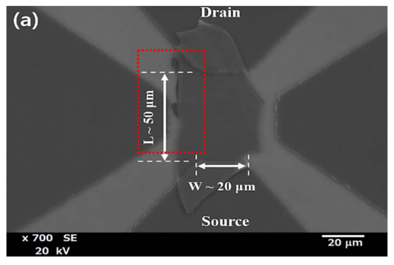
Only a few layers of molybdenum selenide were used to create the devices, totaling to a thickness of about 44 nm. The width and length of the transistor channel were reportedly 50 μm and 20 μm. With the stats in mind, the optoelectronics field can benefit and expand upon its current applications, due to molybdenum selenide’s improved optical absorption compared to MoS2 materials, and its 1.1 3V bandgap.
The full findings of the research can be found in the journal Semiconductor Science and Technology.