The mechanical strain induced on electronic components due to mechanical and thermal stress is an important aspect of their performance consistency and limitations; stress is also used to enable some materials provide critical electronic functions.
Although electronic systems and circuits invoke intangibles such as voltages, currents, power, EM fields, and Maxwell’s equations — to cite a few aspects — they are physically built from mechanical structures called components in the form of transistors, resistors, oscillators, connectors, logic gates, ICs, circuit boards….you get the idea. These components are subject to stresses from various sources, and resultant stain. Digital components are less affected by the nature of the digital world — but only up to the point where parameter values cross certain thresholds. For analog components, stress and its impact are issues which are often a concern, as stress-induced changes in components specifications will affect circuit performance — it is an issue of by how much.
Materials science is a building block of electronic components of all types. This FAQ will look at one aspect of this discipline, namely the fundamentals of stress and strain, and its cause and implications. It will then look at how stress and strain are used, and how they can be both detrimental to component and system performance as well as how it the basis for the functioning of some components.
Q: I see the words “stress” and “strain” used interchangeably. Are they the same?
A: No, they are not. A more formal definition is this:
Strain is the response of a system to an applied stress. When a material is loaded with a force, it produces a stress, which then causes a material to deform. Engineering strain is defined as the amount of deformation in the direction of the applied force divided by the initial length of the material.
Q: What causes stress?
A: It can be caused by basic mechanical loading, or by thermally induced expansion or contraction.
Q: What are the two basic types of stress?
A: Stress can be tensile (stretching, pulling apart) or compressive (squeezed together). The direction of strain is in the same direction as the stress which induced it, for mechanical-loading stress (it’s a little more complicated for thermally induced strain).
Q: What is the fundamental relationship between stress and resultant strain?
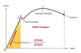
A: A stress/strain graph tells the fundamental story in most cases. This stress/strain curve can take many shapes, depending on the material and the amount of stress (Figure 1). The graph reveals many areas of interest: Young’s modulus, where the stress/strain is reasonably linear; the yield point, at which the material no longer returns to its original dimension; and the fracture point. Some materials have a barely linear relationship with unusual stress//strain curves. However, the curve shown is representative of most materials.
Q: What are the units of the stress/strain measurement?
A: It is the elongation (or compression) dimension divided by the original dimension, so it is unitless. But it also common practice to state it as the ratio of two length units, such as mm per mm or inches per inch, percent, or parts per million (ppm). A measurement might be cited as 10 ppm, or 10 microinches/inch, or 0.001%. For most materials, the strain number is quite small but for others, such as rubber and some plastics, it might be quite large: a 1-cm rubber band which stretches 0.5 cm under the specified applied stress has strain of 50% or 0.5 cm/cm.
Q: How are strain test set up?
A: First, there are well-defined standards for almost every conceivable stress/strain measurement and material, some of which are vendor-specific and many of which are defined by the industry and professional associations such as the ASTM (American Society for Testing of Materials). These test standards define test equipment, set-up, and interpterion of results and span almost every conceivable material and situation, such as steel and adhesives. As a result, tests can be repeated and compared across the industry.
Q: How is the strain itself measured?
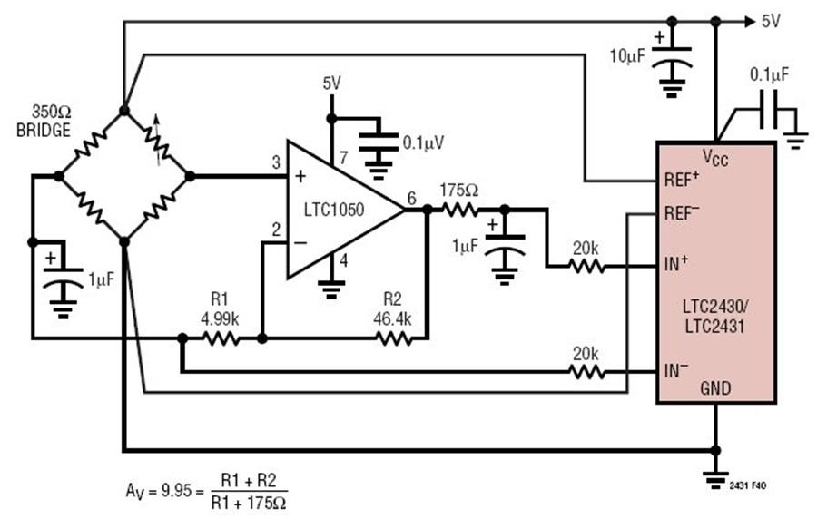
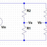
A: There are many ways. The most common is to use a strain gauge (often spelled gage) which is a small component with resistance which varies linearly with its elongation; the nominal resistance of mist commercial strain gages is 120 Ω, 350 Ω, and 1,000 Ω. The strain gage is “excited” by a modest current, on the order of a few milliamperes (to minimize self-heating), and the voltage across it is measured, often using a Wheatstone bridge configuration (Figure 2). The gage is attached to the material under test with a strong adhesive. Strain gages can be quite accurate if used properly. Common nominal resistance values of commercial strain gages are 120 Ω, 350 Ω, and 1,000 Ω.
In some cases, an extensometer is used to measure strain; this is a caliper-like instrument with a strain gage in its body y that can measure with high precision but does not need to be glued to the sample (Figure 3). For cases where the amount to strain is too small to measure with a strain gage, advanced systems such as laser-based interferometers are used, with the movement of the optical interference fringes is observed and can used to calculate tiny, almost infinitesimal amount of strain.

Q: How is the stress applied?
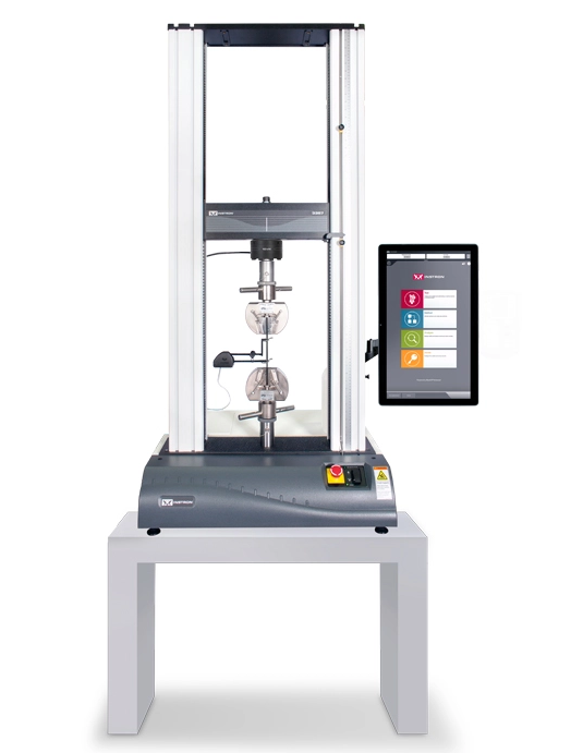
A: It depends on the test set-up. In many cases, a special load frame is used (Figure 4). This is a machine which applies precisely measured amounts of force (load) to the sample under test, while the elongation (or compression) measurement is made. A small frame can produce stress loads to several thousand pounds, while a larger one can deliver tens or even hundreds of thousands of pounds. Note that the “grips” or clamps which hold the sample under test are also complex, highly engineered elements of the test arrangement, and there are specialized grips for nearly every material, type of test, and load range.
In other cases, the material or component under test is heated or cooled in a test chamber, as changes in temperature also represent a source of stress and so induce strain. In fact, these thermal aspects are often a major for passive and active electronic components. Temperature changes speed up or slow down the energy levels of the electrons and molecules, of course. Changes in energy levels affect noise and leakage currents and shift many other parameter values, In addition, the expansion and contraction due to temperature changes can also affect component mechanical dimensions and relationships, and thus electrical performance.
Q: Are these stress/strain tests slow-moving and static?
A: It depends on what attributes are being examined. The rate at which the stress is applied, called the shear rate, is often an important in the test, as nearly all materials are sensitive to it to some extent (Silly Putty is a classic example). For most tests, the first step is a simple single-direction, relatively slow pull or push; in many cases, the test is cycle is then repeated at a slow rate. Higher-rate cycling of these tests is needed for some situations and materials.
Part 2 of this FAQ will look at how stress and strain affect electronic components and how they are the basis for the functioning of some components as well as detrimental to others.
References
The topics of stress, strain, materials science, Young’s modulus, the piezoelectric effect, the Wheatstone bridge, crystal oscillators and filters, and related topics are covered in thousands of online and printed sources. These range from general and less technical to highly technical analyses. Among the EE World references are:
- Filters, Part 2: SAW and BAW devices for RF
- Heat sinks, Part 1: Thermal principles
- Heat sinks, Part 2: Available components
- Wheatstone bridge, Part 1: Principles and basic applications
- Wheatstone bridge, Part 2: Additional considerations
- Quartz crystals and oscillators, Part 1: Crystal basics
- Quartz crystals and oscillators, Part 2: Advanced crystals
- FAQ: Piezoelectric motors, Part 1: actuators
- FAQ: Piezoelectric motors, Part 2: drive circuits
- Solid-state temperature sensing Part 1 — principles
- Solid-state temperature sensing, Part 2 – application


Leave a Reply
You must be logged in to post a comment.