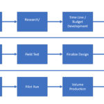
In part 1, we provided an overview of the product life cycle (PLC) and product development cycle (PDC), noting their distinct differences. In this second part, we will explain in detail the 12 steps of the product development cycle (PDC). Figure 1 shows the typical flow chart of a PDC management process and the 12 […]
FAQ
Winning with a sustainable PDC management process in embedded system design (Part 1)
This is the first in a three-part tutorial series explaining how to implement the product development cycle process. Nearly everyone knows Microsoft Excel. Fewer know Lotus 123, and almost no one remembers VisiCalc, the first version of a spreadsheet computer program for personal computers, which ran on the Apple II. There have been a few […]
Simplifying product returns through device security
by Oivind Loe, Chief Technology Officer, Sipsby.com, and Josh Norem, Staff Systems Design Engineer, Silicon Labs Product returns for Internet of Things (IoT) devices can be challenging. On the one hand, connected the device should be locked down as much as possible when going out to the field. On the other hand, when a device […]
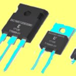
Why it’s tough to characterize SiC power MOSFETs
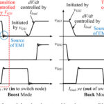
Switching transients and parasitics can combine to thwart the accurate measurement of important MOSFET operating parameters. Levi Gant, Xuning Zhang, Ph.D., Littelfuse, Inc. Silicon carbide (SiC) power MOSFETs get a lot of attention because they can switch fast while maintaining high blocking voltages. But their superior switching qualities also have potential drawbacks. Parasitic inductances caused […]
The difference between CCD and CMOS image sensing
Charge-coupled devices (CCDs) and complementary metal-oxide-semiconductor (CMOS) technology have been in fierce yet friendly competition. Fierce because valuable market share is contested, friendly because the rival digital camera technologies have much in common. It is ironic that the more-costly CCD sensor is used in the most advanced astrophotography instruments and also in low-end point-and-shoot cameras, […]
GaN power devices, Part 2: Application
Part 1 of this FAQ explored the basics of GaN switching transistors at the device and physics level. This part will look at driving and applying GaN devices. Q: What do I need to know to use a GaN device? A: There are three functional blocks associated with power switching: the power-device driver, the power […]
GaN power devices, Part 1: Principles
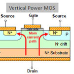
Power devices based on gallium nitride (GaN) are rapidly becoming a viable, higher-performance alternative to silicon MOSFETs due to their higher efficiency and other favorable attributes. In recent years, discrete power-switching and power-handling devices based on gallium nitride (GaN) material have become practical and available, and these devices are now found in many power supplies […]
Testing PV inverters
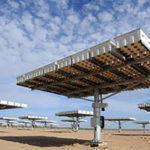
A photovoltaic, or PV, inverter converts the dc output of a solar cell or array into ac that can feed directly into the electrical grid (Grid Tie) or be used by a local electrical grid (Off-Grid). Solar PV inverters have special functions adapted for use with photovoltaic arrays, including maximum power point tracking (MPPT) and […]
Specialized diodes, Part 2: Varactor, Gunn, and PIN diodes
Part 1 of this FAQ reviewed the standard PN semiconductor diode, and looked at some specialized variations called the tunnel, Zener/avalanche, and Schottky diodes. Part 2 briefly explores the varactor, Gunn, and PIN diodes. Q: What about the varactor diode? A: The varactor diode (Figure 1), also called a voltage variable capacitor (VVC) or varicap […]
Specialized diodes, Part 1: Tunnel, Zener/Avalanche, and Schottky diodes
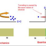
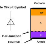
There are diode varieties which do much more than just block current flow in one direction and allow it in the other; some of these special diodes have favorable attributes while others are essential in modern electronics. Every electronic engineer is familiar with the diode: it’s a basic, widely used, two-terminal semiconductor device. The diode’s […]
