The first part of EEWorld’s virtual roundtable discussion considers the challenges of testing power consumption and batteries for wireless IoT nodes and wearables. Joining us for this virtual roundtable are: Janet Ooi (JO), IoT Industry Solutions Lead at Keysight Technologies, Shah Hassan (SH), Business Manager at Tektronix, and Dr. Markus Herdin (MH), Market Segment Manager – Industry, Components and Research with Rohde & Schwarz.
JS: What is the most challenging aspect of testing the very low deep sleep power consumption of wireless IoT nodes and wearables?

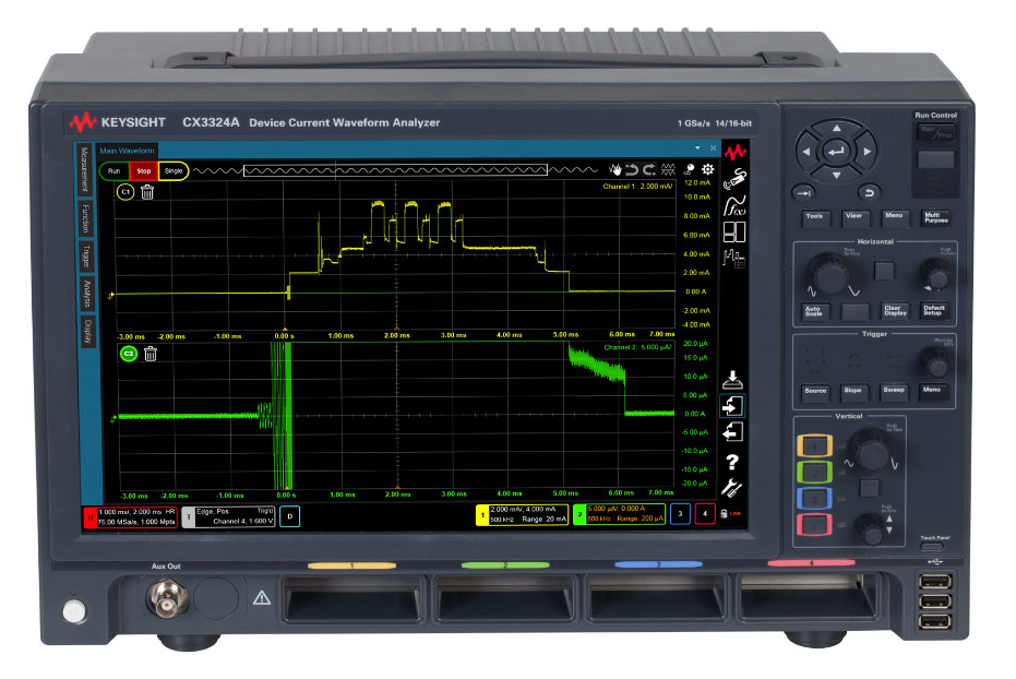
JO: IoT devices, even those as simple as a single wireless sensor node, often have requirements to operate over an extended period of time — sometimes more than ten years. With this requirement and expectation from users, wireless IoT devices need to be extremely energy efficient. Most battery-powered IoT devices have low power sleep modes that consume minimal supply current, often less than 1 μA. However, when the device is in active mode, it might require more than 10 mA. It is challenging to measure such a wide dynamic range of currents with a single measurement.
It is also a challenge when design engineers measure the low-level current of wireless IoT nodes and wearables with clamp-on current probes due to the large noise floor. Using a shunt resistor and an oscilloscope is very useful; however, there is a limit to the minimum measurable current because of the noise floor and the voltage drop across the resistor.
Lastly, there is also a challenge with limited bandwidth. Low-level current waveform measurements with a certain level of resolution require a trade-off with bandwidth. Otherwise, wideband measurements may degrade the resolution. A multimeter or an ammeter is popular for high-resolution measurements but not appropriate for high bandwidth current measurements due to the lower bandwidth.

SH: Generally, for monitoring sleep and/or standby conditions, we are most interested in the current draw characteristics of the circuit design. Yes, over time, there will be some changes in the voltage (with respect to the battery), but with the power load of the circuit being minimal, you are much less likely to witness a noticeable voltage drop. Therefore, it is important that whatever meter you settle on be capable of measuring low current and offer appropriate range scaling to do so.
For instance, the user might think to use an oscilloscope with a current probe. Doable, yes, but at what cost? It will almost certainly have the bandwidth, but if said probe is only offering 1% accuracy, will that be good enough? A Source Measure Unit can act as your supply while also measuring using lower ranges and a high degree of accuracy. For instance, the Source Measure Unit (SMU) may give you a low 10 nA range with 10 fA resolution and 0.1 % accuracy. You could also opt to use a digital multimeter (DMM) supplemented with a power supply. The power supply accuracy may not necessarily be so important, but the DMM specifications are. DMMs provide a cost-effective alternative to the SMU and, in some cases, give you that extra digit of resolution where it is needed. The accuracy may well be given in parts per million (PPM) in lieu of a percentage. There may well be speed and bandwidth advantages for the DMM solution.
One thing to be wary of in either the SMU or DMM setup is burden voltage. If the voltage drop across the internal measuring circuitry is too high, you run the risk of encountering power drop-outs at the device under test. This is more common when monitoring your circuit in high current draw scenarios since higher current measure ranges may be using a larger internal shunt resistance for the given range. However, if the meter in question is enabled with feedback ammeter technology, then the burden voltage can be made much lower.
Speed and type of measurement can be important as well. Oscilloscopes and some DMMs will have digitizing options, which typically lend themselves to faster sampling and tight, consistent timing of measurements. The alternative to digitizing would be an integrated measurement, which tends to be slower as the acquisitions that compose the measurement are averaged and provide a greater degree of accuracy. The user should weigh their instrument selection options so that they get the best piece of equipment that will meet their measurement requirements.
JS: What subtleties do designers need to be alert to when performing multilevel active power testing for system optimization in wireless IoT nodes and wearables?
SH: They need to be aware that fast and abrupt changes with their IoT/wearables systems might disturb the instrument that’s being used to measure it. So they’ll need to consider the DMM or the SMU, for example, that they’re using is suitable for these measurements.
Sleep and standby modes are just a portion of what an IoT-based design will need to be evaluated on. So too are the normal operations and RF transmission modes, which certainly will be where the majority of the power consumption will take place. A sleep mode may be able to operate over long intervals and restrict a device to drawing up to tens of microamps. Conversely, the general operating modes of the device – though ideally less frequent – will exhibit draws in the single-digit up to several tens of milliamps. An RF transmit/receive mode can consume amps of current. Regardless that these general and RF modes are less frequent, the loads that they impose will be the largest contributors to draining a device’s battery.
When we take these types of transitions into consideration, now we have to make sure our measurement instrumentation is also prepared to deal with such conditions. We will want to make sure that we have the appropriate upper ranges and ensure that the measurement resolution can accommodate the large current transitions if the auto-ranging is not fast enough to keep pace. You can find information on range change timing in the instrument datasheets or reference manuals.
JO: Engineers design IoT devices based on use cases and applications, and it is critical that they fully understand the operating profile of IoT devices. For example, the device’s maximum power level, time in standby mode, actively transmitting, receiving data from paired devices, and enabling and disabling peripheral components.
Designers also need to realize their choices in a multiclock architecture — memory, microcontroller unit (MCU) clock speed and firmware programming. These decisions will also affect the charge consumption and system optimization of the IoT devices. With so many subsystems working together in a device and running at different supply voltages, designers need to know when the device will start to fail. For example, it is not always when the battery runs out of power. As soon as the first subsystem fails, the device will fail. This is why designers need to correlate critical RF or DC events of the IoT device to the power consumed, down to the subsystem or event level. Event-based power analysis at different supply voltages gives design engineers quick, visual insights into device behavior and charge consumption. They can then implement strategies to extend the device’s lifetime and measure the effects of those strategies.

JS: What testing architectures and methodologies do you recommend as best practices when dealing with power systems in wireless IoT nodes and wearables?
SH: For power consumption analysis, we recommend hi-resolution 1MS/s current and voltage sampling with sensitivity and visualization to capture all device states. We also recommend a low Noise, quality constant voltage source.
JO: There are several factors to consider when managing power systems in wireless IoT nodes and wearables. Designers must perform extensive design and testing throughout all development processes to ensure the device meets design expectations.
To prevent unnecessary current drain, careful characterization of a device’s dynamic current consumption is critical. Designers must measure low currents accurately and switch to high current measurements quickly and without glitching due to range changes. With the right measurements, the current drain provides a window for gaining additional in-depth insight to optimize battery run time.
Understanding how an IoT device spends its charge when operating in real-world conditions is critical to optimizing battery life. Correlating the device’s current consumption to a specific RF or DC event, also known as event-based power analysis, makes it easier to identify which subsystems or events to prioritize and optimize.
Apart from a typical operating cycle of the IoT device, device designers should perform a stress test on the application features to determine both the device’s true capabilities in the field and its points of failure. Testing the devices in a chamber to simulate varying environmental conditions is also important as batteries might perform differently at various temperature levels.

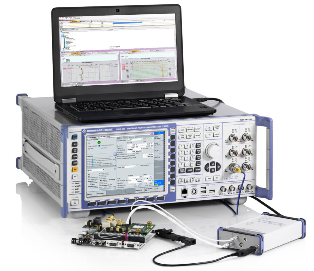
MH: This depends a lot on the actual system and the testing needs. If one is working, for example, with LTE-M or NB-IoT devices, the wireless network must be simulated, as well as the power consumption monitored and optimized. It makes sense to use a setup with a wireless communication tester like the R&S®CMW; equipped with the R&S®CMWrun sequencer software to control running all the power consumption tests, evaluating test results, and reporting; and the R&S®RT-ZVC multi-channel power probe suitable for both very small currents in the μA or even nA range, up to several Amps. Handling such a high dynamic range of 106 or even 109 is not possible with many test devices.
For debugging the embedded electronics of an IoT device, the combination of an R&S®RTE or R&S RTO oscilloscope with the R&S®RT-ZVC probe provides multi-domain debugging, effectively correlating electrical signals of the IoT device with power consumption to optimize battery life.
In low-cost applications where test costs must be kept to the minimum, a power supply with powerful functions for simulating battery performance like the R&S NGM200 is the right tool. It provides a clean source of power for the IoT device while being able to simulate the battery as well as to measure the current consumption. With the high-speed FastLog function, run measurements on voltage and current at intervals as short as 2 microseconds (at acquisition rates up to 500 kSample per second).

JS: How do the challenges of measuring long duration but very low power consumption compare with the challenges of measuring very brief high current spikes in these devices?
JO: IoT devices sleep at lower current levels and for extended periods to prolong battery life. This process has caused device characterization to be lengthier since it must go through a series of operation cycles. Apart from measuring very low current, the instrument will need to log and analyze substantial amounts of data from file sizes ranging from hundreds of GB to TB. If the sampling rate is too fast, the total file size might not be realistic.
When powered on or actively transmitting, IoT devices will see quick changes of current, from low to very high current spikes, such as inrush current. The instrument used for device characterization will need to accurately capture and measure the dynamic current changes to validate circuit designs. Inrush current has a high bandwidth. Designers will require instruments with high sampling rates to capture these fast signals accurately.
To overcome these challenges, designers will want an instrument that can capture dynamic current changes, have a high sampling rate, store and play back data from storage for analysis.
SH: The challenge with measuring a long duration but very low power consumption is how much data is being captured and saved into the memory of the instrument. The user might choose to stream the data into the PC for a very long duration of testing.
On the other hand, the challenge with measuring the very high current spikes would depend on the instrument’s current ranges and resolution to capture these fast spikes.
JS: Thank you to our three Virtual Roundtable participants for their insights into Testing power consumption and batteries for wireless IoT nodes and wearables! You might also be interested in reading Part 2 of this Virtual Roundtable, where our panelists will delve into the challenges and nuances of complementary cumulative distribution function (CCDF) testing and predicting actual battery performance.


