LED’s and photovoltaic cells play increasingly prominent roles in our world. Both are semiconductor diodes. The LED or light-emitting diode emits light while the photovoltaic cell converts light to electricity. The LED is a diode that emits light only when forward-biased. Under a forward voltage bias, electrons cross from the n-region and recombine with the holes in the p-region. Free electrons are in the conduction band of semiconductor energy levels, while holes are in the valence energy band. Thus the energy level of the holes is lower than the energy levels of the electrons. Some portion of the energy must be dissipated to recombine the electrons and the holes. This energy is emitted in the form of heat and light.

LED charge carrier behavior as explained in Wikipedia.
In ordinary silicon and germanium diodes, electrons flowing through the diode dissipate energy in the form of heat. But in diodes composed of gallium arsenide phosphide (GaAsP) and gallium phosphide (GaP), the electrons dissipate energy by emitting photons. If the semiconductor material is translucent, the diode junction becomes a source of light, thus creating a light-emitting diode.
The recombination of electrons and electron holes in the LED produce light via electroluminescence. The wavelength of the light produced depends on the energy band gap of the LED semiconductors. Most of the light produced tends to reflect back from the surface of the semiconductor (high index of refraction), so LEDs use special optical coatings and die shapes to boost light emission.
In modern-day LEDs, materials such as gallium arsenide with various trace doping elements are used to produce different colors of light. Another type of LED uses a quantum dot which can have its properties and wavelength adjusted by its size.
LEDs are usually built on an n-type substrate, with an electrode attached to the p-type layer deposited on its surface. P-type substrates, while less common, ae used as well. Many commercial LEDs also use a sapphire substrate.
The first LEDs were used in TV remotes, emitting a low-intensity, narrow infrared beam sufficient only to be sensed a few feet away. Over the years they evolved, first becoming primitive indicator lamps and then seven-segment displays. (Engineers who were in school during the early 1970s, when LEDs first became commercialized, can recall lab sessions where undergrads peered in at a dimly lit LED which was part of a circuit set up by lab instructors. Back then, LEDs weren’t entrusted to mere undergrad engineering students.)
You might think the idea for LEDs came along shortly before their commercial debut. Actually, in 1907, Henry Joseph Round observed luminescence in a solid-state diode, using a cat’s whisker silicon carbide detector. Two decades later, a Russian investigator, Oleg Losev created the first true LED. Georges Destriau observed electroluminescence when he applied an ac voltage to zinc sulfide (ZnS) powder suspended in an insulator. In 1955, Rubin Braunstein in RCA Labs, observed infrared emission in gallium arsenide (GaAs) and other semiconductors. Additionally, he reported room-temperature infrared emission in diodes using gallium antimonide (GaSb), GaAs, indium phosphide (InP) and silicon germanium.
James Beard and Gary Pittman, working at Texas Instruments, placed a tunnel diode on a GaAs substrate, producing near-infrared emission. Subsequently, they observed light emission as well as signal transmission between a GaAs P-N light source and a semiconducting photodetector. Soon Texas Instruments began making infrared diodes and LEDs that used GaAs crystals emitting 890 nm light beams.
At General Electric, Nick Holonyak build the world’s first visible red LED. Then, George Craford in 1972 demonstrated a yellow LED and greatly increased the intensity of red and orange LEDs.
Early LED’s played a role in laboratory test equipment, but they were still too costly, in excess of $200 per unit, for general usage. That changed when Mohamed Atalla, renowned MOSFET inventor, and his associates at Hewlett Packard collaborated to develop new LEDs using GaAs, GaAsP and InAs devices. In the 1970s, Fairchild Optoelectronics produced LEDs priced below five cents each, based on Atalla’s surface passivation technology. But LED colors other than red and some other narrow-band hues remained elusive. Blue LEDs and laser diodes were too dim and gallium nitride devices were discontinued until, in 1989, a semiconductor manufacturer based in North Carolina introduced a commercially available but inefficient blue LED based on an indirect bandgap semiconductor, silicon carbide (SiC).
High-intensity blue LEDs emerged in 1991. Subsequent bright blue LED improvements made Blu-ray a reality. The quest for high-intensity white LEDs gave rise to a red-green-blue mix that the eye perceives as white, with incrementally improved color rendition.

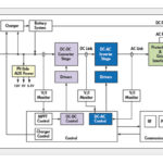
An ideal solar cell is often modelled as a current source in parallel with a diode. Because no solar cell is ideal, a shunt resistance and a series resistance component are generally added to the model.
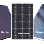
That brings us to another type of diode commonly known as the photovoltaic or solar cell. The most common solar cells are based on silicon and are configured as large-area p-n junctions. Here, current, voltage and resistance change upon exposure to the sun’s rays. The most frequently-installed single-junction crystalline silicon solar cell exposed to direct sunlight produces a maximum open-circuit 0.5 to 0.6 V.
When a photovoltaic cell absorbs a photon, the photon energy is given to an electron in the crystal lattice. Usually this electron is in the material’s valence band. The energy given to the electron by the photon “excites” it into the conduction band where it is free to move around within the semiconductor. The network of covalent bonds that the electron was previously a part of now has one fewer electron. This is known as a hole. The presence of a missing covalent bond allows the bonded electrons of neighboring atoms to move into the “hole”, leaving another hole behind, thus propagating holes throughout the lattice. It can be said that photons absorbed in the semiconductor create electron-hole pairs.
A photon only needs energy exceeding that of the band gap to excite an electron from the valence band into the conduction band. However, much of the solar radiation reaching the Earth is composed of photons with energies exceeding that of silicon’s band gap. The solar cell absorbs these higher energy photons, but the difference in energy between the photons and the silicon band gap is converted into heat rather than electrical current.
We should also mention a new kind of photovoltaic cell made of perovskites, named after the mineral with that specific crystal structure. Like silicon solar cells, perovskite solar cells are diodes. Their unique crystallographic structure makes them highly effective at converting photons of light from the sun into usable electricity. The most common perovskite solar cell (PSC) uses a hybrid organic-inorganic lead or tin halide-based material as the light-harvesting active layer.
The benefit of perovskite solar cells is that they can convert ultraviolet and visible light into electricity efficiently, whereas crystalline silicon is most efficient at converting infrared light. So there is a lot of research into fabricating solar cells that are hybrid combinations of the two materials.
The problem with perovskite cells is a short life. Most cells demonstrated so far degrade after a few months. That said, a UK start-up called Oxford PV hopes to start selling its perovskite-silicon cells to the public in early 2022. The firm says its data suggest that in terms of life time, the cells will perform about the same as commercial silicon panels.