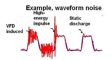
Electronic noise and jitter are closely related phenomena, but they are not the same. While noise typically manifests as amplitude distortion, jitter pertains to timing of digital signals. Either of them can be caused by outside interference or internal sources. Noise can be seen in an oscilloscope time domain display as a noticeable thickening of the trace and in the frequency domain display as a prominent, roughly horizontal fluctuating line known as the noise floor. Normally, the signal of interest sits above the noise floor. If it falls below the noise floor, the signal is no longer intelligible, lost in a sea of random energy. For this reason, manufacturers strive to lower the noise floor in their instrumentation.
A key metric is the signal to noise ratio (SNR). High SNR is good, low SNR is bad. A high level of noise and/or low signal-strength reduce the SNR. As the signal weakens, the oscilloscope autoset–or automatic gain control in a radio or TV–boosts the amplification in an attempt to retain the signal. But noise is also amplified – hence snow and audible noise when the receiver is tuned to an inactive channel.
Types of electronic noise are:
Thermal (also known as Johnson-Nyquist) noise. This is unavoidable, although there are techniques to mitigate it. Thermal noise is present in all conductors, regardless of whether they are connected to a power source. Thermal noise is also generated within passive and active components. In an oscilloscope, these, along with external cabling and the equipment being tested, all contribute to the total noise load. Thermal noise is generated by the thermal motion of charge carriers. A form of white noise, its spectral density is essentially uniform throughout the frequency spectrum. For this reason, it can be reduced in an oscilloscope by temporarily limiting the bandwidth (not of the instrument, but of the signal) provided the signal is not in the process truncated.
Shot noise. This is due to random fluctuations of electrical current crossing an impedance discontinuity, such as the barrier in a diode. This is because pieces of the signal arrive at the far end at different times.
Flicker noise, unlike thermal noise, diminishes at higher frequencies, and it cannot be eliminated by bandwidth limiting.
Burst noise. This is caused by random abrupt current or voltage changes. It is perceived in audio equipment as popping or crackling sounds.
Transit-time noise. This is a problem at higher frequencies, VHF and beyond. It arises in transistors when the time for electrons to travel from emitter to collector is close to the period of the signal of interest. At still higher frequencies, its amplitude rises so this noise eventually dominates all other noise.
These are all noise sources that originate within test instruments or connected cabling and equipment. There is also coupled noise, from an external source. The principal types are intermodulation noise, crosstalk, interference, atmospheric noise, industrial noise, solar noise and cosmic noise.
Besides bandwidth limiting and signal averaging, the principal coupled noise mitigation methods are the use of a Faraday cage, avoiding capacitive coupling, avoiding ground loops, shielding cabling, physical distancing, twisted-pair wiring, and notch (band rejection) filters.
Dither is a noise mitigation strategy consisting of the intentional introduction of additional noise to reduce noise in the bandwidth of interest. Another strategy is active noise control by means of noise cancellation.
Digital circuitry is more resistant to noise than analog circuitry unless the noise is excessive to the point of overwhelming the pulse train. This is because digital signals at any instant are either high or low and remain so without regard to background noise. In troubleshooting digital signals, it is a good idea to begin by examining them via oscilloscope analog channels to detect any gross distortion that may be problematic.
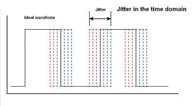
Jitter, like noise, is almost always harmful. (Both are occasionally used in electronic music.) Rather than random variations in amplitude as in noise, jitter consists of timing deviations from the intended signal, generally in a digital pulse stream. It is particularly relevant in digital-to-analog conversion, serial digital communications, phase-locked loops and clocks in computers and related equipment. The principal types of jitter are:
Absolute jitter, which is the difference in location of a signal’s edge with respect to its ideal position. This is the generic form of jitter and the others are variations.
Period or cycle jitter, which is the difference between an intended clock period and its actual average. It plays a prominent role in synchronous circuitry where the shortest clock period places limitations on error-free operation. Thus, the average clock period impacts circuit performance. The aspiration is to reduce period jitter so as to synchronize the shortest to the average clock period.
Cycle-to-cycle jitter is defined as the difference in duration between successive clock periods.
The unit interval (UI) is used to measure jitter as a fraction of each period. Picoseconds are used in microprocessor technology, while engineering textbooks refer to degrees and user-friendly radians.
Jitter distribution may Gaussian or non-Gaussian. Gaussian distribution jitter is best quantified in terms of standard distribution, an RMS measurement for zero-mean distribution. In contrast, jitter that is caused by power-supply noise or a similar outside phenomenon, will have a decidedly non-Gaussian distribution. Peak-to-peak measurements are suitable in these instances.
A different sort of jitter appears in computer networking and telephony. It is packet delay variation. This delay spans the beginning of a transmission at the source to the beginning of its reception at the destination. Instantaneous packet delay variation consists of the temporal difference between successive packets. The two varieties are known as dispersion and clumping. Either of these is harmful and inconvenient to the user in voice over IP (VoIP). Packet delay variation in multimedia streams has been successfully mitigated by the installation of a properly-sized buffer at the receiver. This technique depends upon adequate bandwidth and sufficient buffer size.
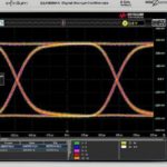
High clock frequencies require more sophisticated techniques in testing for jitter and measuring its impact. Eye patterns are used to good effect. Because the eye openings are smaller at higher frequencies, jitter is subject to tighter tolerances. It should be noted that to display eye patterns, an oscilloscope must have higher than usual specifications. If an instrument is to be purchased for this purpose, first check with the manufacturer’s application engineer.
The procedure is to apply the digital signal of interest to an oscilloscope vertical input, simultaneously using the data rate to trigger the horizontal sweep. As successive cycles are acquired, the eye pattern becomes more cluttered if there is significant jitter. A distortion-free signal will yield a simple eye pattern that looks like a Paul Klee rather than a Jackson Pollack.
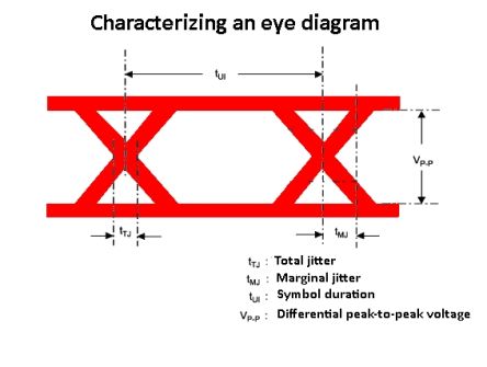
The pattern on the oscilloscope display resembles one or more eyes peering between a lower rail, representing logic 0 and an upper rail resembling logic 1. When persistence and other oscilloscope settings are properly adjusted, the eye pattern reveals the presence of jitter. Minimal signal distortion manifests as an open eye pattern, while noise and inter-symbol interference cause the eye to close since with the passage of time, unconstrained traces accumulate.
Jitter measurement in serial bus circuits is expected to conform to standards, which cover jitter tolerance, jitter transfer function and jitter generation. Jitter mitigation is required in equipment maintenance as well as in new product development. One technique is to implement anti-jitter circuits in conjunction with the clock. Output pulses are retimed to resemble ideal clock performance.
A dejitterizer uses an elastic buffer to temporarily store the signal, then retransmit it at a rate compatible with the incoming signal. Another jitter mitigation technique consists of installing a filter to minimize sampling jitter.
A principal cause of jitter in the output of oscillators is drifting with respect to time, temperature and supply voltage. For sensitive measurements as in a spectrum analyzer where you are working close to the noise floor or in a vector network analyzer prior to field calibration, it is prudent to warm up the instrument for a half hour or so, and operate it in a thermally stable location.
A phase-locked loop generates a signal whose phase relates in a uniform manner to the phase at the input. For this reason, phase-locked loops are resistant to jitter, especially when caused by variations in the power supply and ground lines.