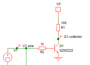
While we are all probably familiar with the concept of capacitors storing charge, remember that semiconductors do so as well. This may not be an issue for your design or it could be a major headache, depending on the application. With bipolar transistors, charge storage in the base when the transistor is saturated will slow down turning the transistor off. Take the following simple example:
The switch on and off waveform is shown below with the driving waveform at the top of the graph:

While switch on is quick, turning off takes around 250ns due to the excess base current causing charge storage in the base. That charge needs to be removed before the transistor can turn off. One speedup method is a capacitor across the base resistor. An other is a Schottky diode from base to collector. The Schottky diode prevents the excess base current going into the transistor base once the transistor is fully turned on and diverts the excess base current through the diode instead of the base. These two options are shown below.

The difference in the turn-off time is easily seen. The blue trace is with the speedup capacitor and the green trace with the Schottky diode. The magenta trace is the original.
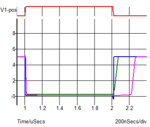
While the speedup capacitor looks the best (i.e. fastest) there are some caveats. Firstly, the driving waveform must be able to supply the extra current required – you are bypassing the base current limiting resistor with the capacitor. In the example shown the peak current in the capacitor is 60mA to 80mA. Also, there is a small “kick” in the output voltage which takes it negative – just visible on the blue trace. This is caused by the capacitor pulling the base below 0V when the driving voltage drops to zero. This may or may not be an issue with your application.
The use of a Schottky diode is often not quite as good as you might hope because, while they don’t have significant charge storage problems, they still have capacitance and store charge so can slow things down a little, particularly if the diode is larger than needed for the application.
MOSFETs are another area where there can be significant charge storage which can cause problems. Analog switches, which are simply a P and N type MOSFET in parallel, will exhibit charge injection when they are switched off. If you are using the analog switch to sample a signal on to a capacitor (in a “sample-and-hold” circuit) then the charge injection will cause an error in your sampled voltage depending on the charge injection and sampling capacitor value. Another cause of such an error is the feedback capacitance which couples the gate voltage to the drain. Both the effects of charge storage and feedback capacitance can affect the on/off switching speed in power MOSFET applications as well.

The performance of this simple switching circuit looks fine when you look at the drain voltage, but slow. When you look at the gate voltage you can see some of the cause of the slow turn-off. When the transistor starts to actually turn off the voltage on the gate itself doesn’t follow the driving voltage at the other side of the resistor. The gate voltage pretty much hits a plateau, slowing down the switch off. This is due to the combination of the charge storage and gate-drain feedback capacitance. In this case the effect of the feedback capacitance is to couple back from the drain and prevent the gate voltage from dropping. The charge storage is also preventing the gate voltage from dropping quickly – the charge is being removed. In the case of a sample-and-hold type circuit, the feedback capacitance is really causing a problem feeding forwards – the gate voltage change is altering the drain voltage rather than the other way round in this circuit.


Leave a Reply
You must be logged in to post a comment.