by Aijaz Fatima, Mentor, a Siemens business
We live in a shrinking world, and like so much else, the size of ICs is shrinking too. The small size of an IC has many advantages, but it increases the power density of the IC, which leads to many concerns. An IC with a high power density not only heats up end products, but also wears out early. The IEEE 1801 low-power standard helps you create reliable, robust, and standardized designs that mitigate these issues.
Once you have developed a robust low-power design, you need to verify it. Verification engineers are turning to sophisticated low-power simulators to ensure that their designs are functionally and behaviorally correct and follow the IEEE 1801 low power standard, commonly known as the Unified Power Format (UPF). One such simulator is the Questa Power Aware (PA) simulator from Mentor, a Siemens Business. This article uses Questa PA as an example of the various types of low-power checks that simulators can perform on low-power RTL and gate-level designs.
Before performing any low-power check, you must provide complete information about your design’s power domains and the dependency of any two connected power domains in the UPF file; otherwise, the simulator will not be able to examine these power domain crossings and will erroneously report them as Not Analyzed crossings.
Classification of Low-Power Checks
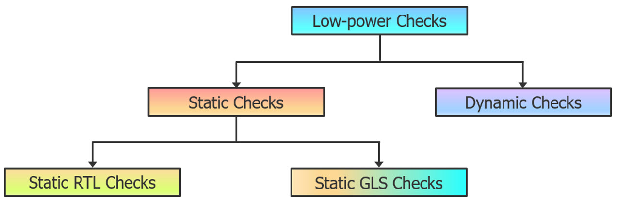
Static Checks
Static checks detect architectural issues in the design, such as a missing isolation or level shifter cell. Because static checks can be performed without running a simulation, they save time and effort as you do not need to write a testbench. So you can run them on your low-power design as soon as the design is ready.
There are two kinds of static checks: static RTL and static gate-level simulation (GLS) checks. The static RTL checks are run on RTL designs and static GLS checks on gate-level designs.
Dynamic Checks
Dynamic checks are performed on the design while running simulation. Dynamic checks detect behavioral issues in the design, such as incorrect power sequencing of power domains.
Classification of Static and Dynamic Checks

Isolation Checks
Let’s consider a that design has two power domains, PD_1 and PD_2, and a signal, s1, propagates from PD_1 to PD_2, as shown below:

During normal working conditions, that is when both power domains are powered-up, the signal s1 has either a 0 or 1 value. But when the power domain PD_1 is powered-down and PD_2 is powered-up, the value of signal s1 is unknown. This corrupts the powered-up logic in the PD_2 domain.
To avoid this, design engineers place isolation cells between the outputs of the powered-down domain and the inputs of the powered-up domain:

During normal working conditions, the isolation cell works as a buffer. However, when PD_1 is powered-down, the isolation cell clamps its output to either a 0 or 1 value. The isolation cell has an isolation enable signal that determines whether the isolation cell should provide isolation or work as a buffer.
Most designs have multiple power domains with numerous signals crossing these domains, which may lead to many isolation issues. The simulator runs various isolation checks on the design to find any isolation issues and flags an error in case of a violation.
A few cases when the simulator will flag an error are listed below:
- An isolation cell is required for a crossing, but it is neither present in the design nor specified in the UPF file.
- An isolation cell is not required for a crossing, but it is either present in the design or specified in the UPF file.
- An isolation cell is present in the design, but the corresponding strategy is not defined in the UPF file.
- An isolation strategy is specified in the UPF file, but an isolation cell is not present in the design.
- Two different clamp values are specified for an isolation cell in the UPF file.
- The isolation clamp value is different from the reset value of the flop.
- The clamp value of the isolation cell in the design does not match the corresponding strategy specified in the UPF file.
- The location of the isolation cell in the design does not match the location specified in the UPF file.
- The isolation control signal is not generated from an always-on region, or is unconnected, floating, or driven by constants.
- The isolation enable signal specified in the UPF file reaches the data pin of the isolation cell or does not reach the enable pin of the isolation cell.
- For an internally isolated IP pin, an isolation cell is present in the design or is specified in the UPF file.
- The isolation control signal is disabled when the source domain is powered-down and the sink domain is powered-up or when the source domain is in a CORRUPT state and the sink domain is not in a CORRPUT state.
- The isolation control signal is active when there is no requirement for isolation.
- The value at the output of an isolation cell is different from that at its input during normal working conditions.
- The value of the isolated port changes during the active isolation period.
Also, the simulator will use notation to flag valid scenarios, such as when a valid isolation cell is specified in the UPF file.
Level Shifter Checks
Now we will consider a design with two power domains, PD_3 and PD_4, and a signal, s2, propagates from PD_3 to PD_4, as shown below:
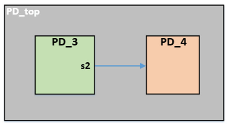
When both of the power domains are powered-up, and the voltage difference between the power domains is less than a threshold value (which you can set in the simulator), there are no issues in the design. However, if the voltage difference is greater than the threshold value, let us say PD_4 is operating at a higher-voltage level than PD_3, then a logic 1 at PD_3 can be assumed a logic 0 at PD_4. This leads to incorrect data transmission.
To avoid this, design engineers place level shifter cells between the power domains.
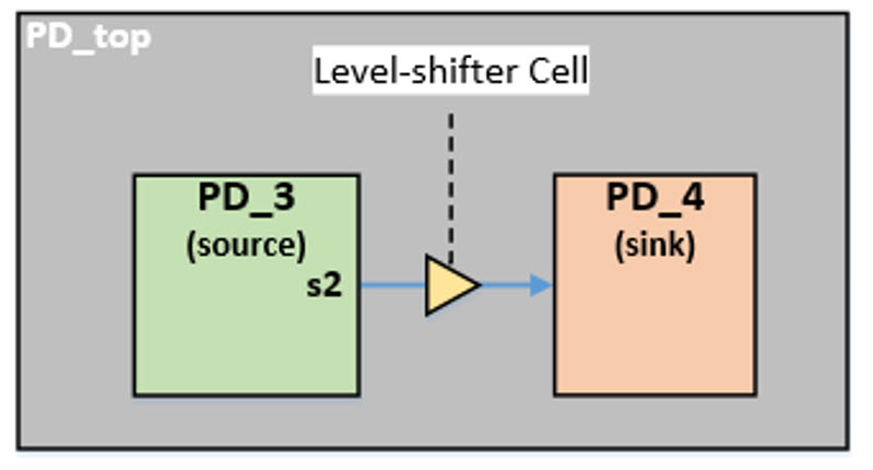
The level shifter cells convert high-voltage levels to low-voltage levels and vice versa. This enables correct data transmission between two different power domains. Similar to an isolation cell, a level shifter cell has a level shifter enable signal that determines whether the level shifter cell should convert the voltage levels or should work as a buffer.
A level shifter cell can be of the following two types:
- High-to-Low – Converts a high-voltage level to a low-voltage level. It is inserted when the source power domain operates at a higher voltage and the sink power domain operates at a lower voltage.
- Low-to-High – Converts a low-voltage level to a high-voltage level. It is inserted when the source power domain operates at a lower voltage and the sink power domain operates at a higher voltage.
A design may have multiple power domains whose voltage difference is greater than the threshold value, which may lead to many level shifter issues. The simulator runs various level shifter checks on the design to find out the level shifter issues and flags an error in case of a violation.
A few cases when the simulator flags an error are listed below:
- A level shifter cell is required for a crossing, but it is neither present in the design nor specified in the UPF file.
- A level shifter cell is not required for a crossing, but it is either present in the design or specified in the UPF file.
- A level shifter cell is present in the design, but the corresponding strategy is not defined in the UPF file.
- A level shifter strategy is specified in the UPF file, but a level shifter cell is not present in the design.
- The direction of the level shifter cell specified in the UPF file is not correct. For example, instead of a high-to-low level shifter cell, a low-to-high level shifter cell is specified.
- The location of the level shifter cell does not match with the location specified in the UPF file.
Also, the simulator will use notation to flag valid scenarios, such as a valid level shifter cell is specified in the UPF file.
Retention Checks
Consider you have a power domain, PD_5, which is powered-down. When the domain is powered-up again, all the state information from before the domain was powered-down is lost. To avoid this, designers place retention cells in power domains, which stores the state value of the power domain. Retaining the state value helps the power domain become operational sooner.
A design may have multiple power domains that are powered-down, which may lead to many retention issues. The simulator runs various retention checks on the design to find out the retention issues, and flags an error in case of a violation.
A few cases when the simulator flags an error are listed below:
- A retention cell is required, but it is neither present in the design nor specified in the UPF file.
- A retention cell is not required (as the power domain is an always-on domain), but it is either present in the design or specified in the UPF file.
- A retention cell is present in the design, but it does not have the corresponding strategy defined in the UPF file.
- A retention strategy is specified in the UPF file, but a retention cell is not present in the design.
- The retention condition is not asserted when the power domain is powered-down.
- The retention control signal is not generated from an always-on domain, or is unconnected, or is driven by a constant.
- The retention condition is disabled at power down or power up.
- The retention condition toggles at power down.
Again, the simulator uses notation to flag valid scenarios, such as a valid retention cell specified in the UPF file.
Back-to-Back Checks
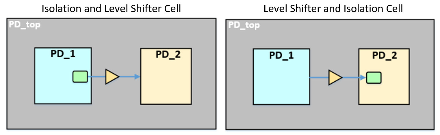
Sometimes your design has back-to-back cells, which might be any of the following types:
- Isolation and level shifter cell
- Level shifter and isolation cell
- Isolation and isolation cell
- Level shifter and level shifter cell
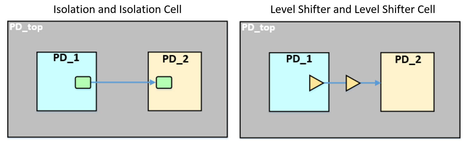
The simulator identifies and reports these back-to-back cells. It also reports back-to-back isolation cells with the same, different, or unknown control signals and back-to-back isolation cells with the same or different clamp values.
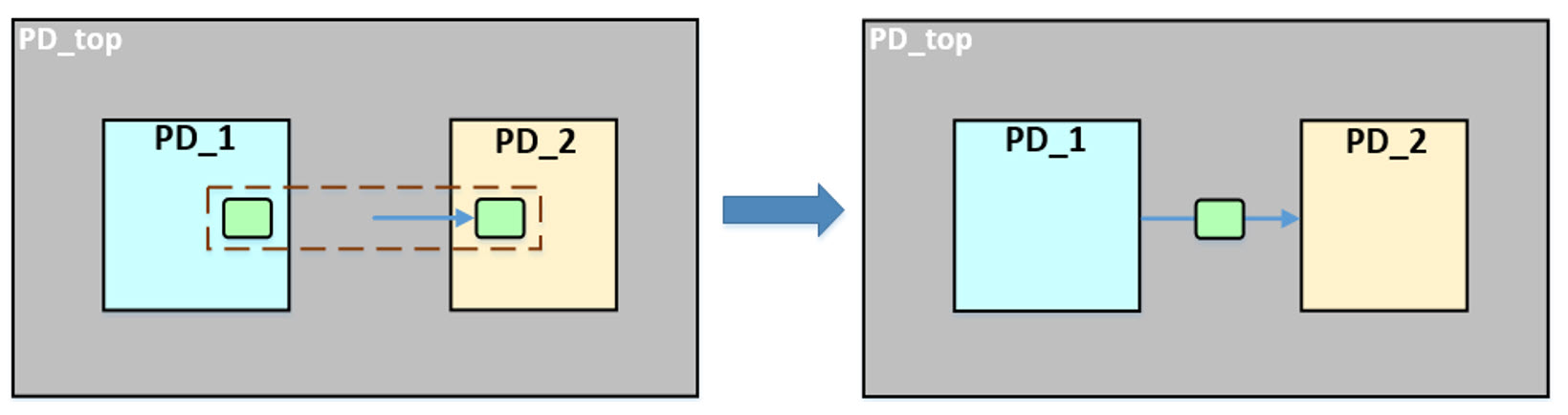
If the cells are of the same type (isolation and isolation or level shifter and level shifter), then you can replace the cells with a single cell, as shown here:
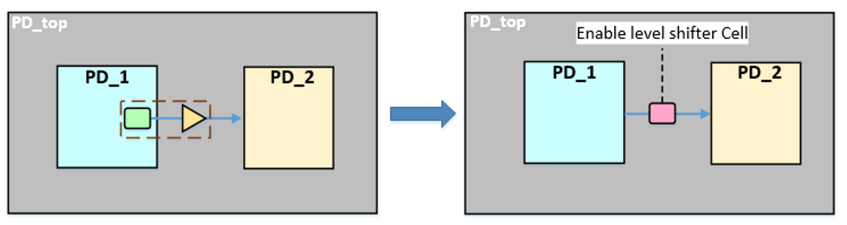
If the cells are of different type (isolation and level shifter or level shifter and isolation), then you can replace them with a single cell called an enable level shifter cell, which functions both as an isolation and level shifter cell. An enable level shifter cell occupies less space than having both an isolation and level shifter cell.
Miscellaneous Checks
The simulator performs various other checks to ensure that your low-power design is reliable and robust.
A few cases when the simulator flags an error are listed below:
- The design cells have missing liberty attributes.
- The isolation, level shifter, or retention supply is powered-down during the active isolation, level shifting, or retention period.
- The power signal of a power domain gets corrupted.
- The input of a power domain toggles when the power domain is powered-down.
- The power state table or the supply port reaches an illegal or undefined state.
Conclusion
It is very difficult to manually find each and every low-power design issue. Advanced low-power simulators, such as Mentor’s Questa Power Aware simulator, help you to identify and report low-power issues and provide a bug-free design. With every release, you will find new low power checks in the simulator that will make your life easier!


Leave a Reply
You must be logged in to post a comment.