Duane Benson, Chief Technology Champion at Screaming Circuits
Via in pad seems to be one of the hot topics these days. It’s a bit of a tough one too. The SMT guys pretty much always say, “don’t ever do it.” However, with certain parts, the  component manufacturer strongly recommends it. You gotta love those mutually exclusive requirements. Rather than just telling you “no, never” here’s a few guidelines on how to do it properly.
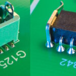
PCB assemblers don’t like it, but with some designs, if done properly, there can be a number of compelling reasons for putting vias directly in the SMT pads for BGA and QFN packaged components.
- It can make routing easier with big or fine pitch BGAs
- It can allow really close placement of bypass capacitors
- It can help with thermal management
- It can help with grounding on high-frequency parts
The primary reason we don’t want to see vias in pads is that when left open, those via holes act like little capillary straws and suck solder off of the pad. A couple of undesirable events can happen depending on the method used during board fab.
- If your vias are left open, solder will tend to wick down into the via hole. The larger the diameter, the worse the wicking problem can be. You might end up without enough solder left to secure the component, or even a solder bump on the bottom side of the board which could interfere with other components or lead to shorts.
- If your vias are capped or partially filled, the caps might pop off due to thermal expansion or out-gassing. Internal air bubbles can migrate up, leading to voids in your solder joint.
Open vias in pads are not an industry-accepted practice. In a perfect world, we’d like to never see one. However, the real-world is saying otherwise. Manufacturers of QFN parts are starting to recommend vias in the heat-slug pad for improved thermal conductivity. High-frequency designs benefit from the shortest possible routing, which may indicate via in pad. Superfine pitch BGAs may not leave any other options.
My first recommendation would be to re-design the boards so the vias are in between the pads, plug or cap the vias at the board house or to use microvias that don’t go all the way through the board. If you can’t do any of that, use as small a diameter as the design will allow and follow the component manufacturer’s guidelines for placement and via capping or filling.


Leave a Reply
You must be logged in to post a comment.