Understanding the role and implications of impedance in RF transmission lines and antennas is vital to successful system performance.
The traditional matching approaches are still in wide use, but new application requirements and advances in components, modeling and simulation, and manufacturing precision have also provided new ways to address the matching problem.
Q: What is this different approach to building new matching solutions?
A: It involves using the PC board itself in either microstrip or stripline configuration to create matching sections and circuits.
Q: What’s the difference between microstrip and stripline on a PC board?
A: Microstrip line routing is a transmission line trace routed on an external layer of the board (Figure 1). Because of this, it is separated from a single ground plane by a dielectric material. Stripline is a PCB transmission line trace surrounded by dielectric material suspended between two ground plane layers within a printed board.

Q: What are the relative attributes of microstrip and stripline?
A: Microstrip routing has better signal characteristics than stripline because the transmission line is on the surface layer of the board. Board fabrication is also less expensive with microstrip since the layer structure of one plane, and one signal layer makes the manufacturing process simpler. Stripline can be more complex to manufacture because it requires multiple layers to support the embedded trace between two ground planes. However, the width of a controlled impedance trace in a stripline is less than an impedance trace in a microstrip of the same value. This is because of the second ground plane. These smaller trace widths enable greater densities, which in turn enables a more compact design.
Q: So, how do microstrip and stripline apply to matching needs?
A: Using precision PC layout and fabrication to tight tolerances using materials with known and consistent properties., it is possible to create the needed matching circuitry, whether as quarter-wave transmission-line matching circuit or even an LC circuit. The PC board copper can be configured to provide the necessary conductor dimensions and even provide inductances and capacitances for the matching. In this case, stray and parasitic values, which are normally sources of error and problems, can be turned to advantage and used for the needed L and C values.
Q: Can you show an example?
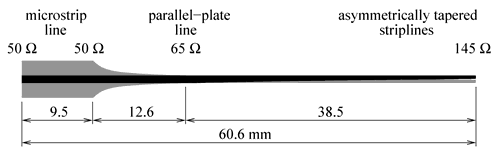
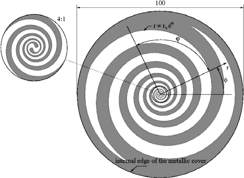
A: Figure 2 is just one of many examples. In some cases, microstrip/stripline topologies are used to match onboard PC trace or component impedance to board connectors. They can also be fabricated as part of a stripline/microstrip plus antenna arrangement, Figure 3.
Q: What are the benefits of using the microstrip or stripline approach?
A: First, it is “free” as there is no component on the bill of materials (BOM) to add cost. Second, it allows for unprecedented flexibility in approaches to implementing impedance matching. In fact, it can be used to create matching circuits that cannot be realized using discrete components and multiband matching circuits with integral filtering. Finally, the matching circuits can be integrated into the antenna if a PC board antenna is used, leading to the pair’s tightly coupled, compact performance.
Q: If microstrip and stripline approaches have all these benefits and can almost be considered as “something for nothing,” what are the drawbacks?
A: It requires PC board space for the matching circuit itself, and such space is often at a premium, so it might be better to locate the matching circuit off-board and near the antenna. Even if required space is available, nearby components can affect performance, and so a “guard zone” must be established. It also requires very careful modeling and simulation of the electromagnetic situation to create and verify the performance, and any shortcomings in modeling – especially of strays and parasitics – can cause large errors in this process.
In addition, it requires very tight control of the PC board material, fabrication process, and dimensions – even the minute surface roughness of the copper cladding affects performance, as does dimensional accuracy of the copper cladding and substrate. Finally, the subtle electrical parameters of the copper and substrate have to be known and modeled, including (but not limited to) conductivity of the copper, dielectric constant and losses for the substrate, and the temperature coefficients of each must be included in the model and simulation as well.
Conclusion
Impedance matching and VSWR are critical issues in wired RF circuits, both interstage and between antenna and system. There are countless resources available which discuss them with perspectives spanning electromagnetic theory and deep math to somewhat simplified analysis and with practical approaches from volume manufacturing to one-of-a-kind custom approaches.
Related EE World Content
What are the functions and principles of S-parameters (Part 1)?
What are the applications and measurements of S-parameters? (Part 2)
RF power amplifier, Part 1: Functions and Elements
Solar cells and power, Part 2 – power extraction
Measuring antenna properties
Using the Smith chart for Impedance matching, Part 1
Impedance matching and the Smith Chart, Part 2
The difference between SWR and TDR meters
Measure power in complex RF signals
What are RF waveguides? Part 1: context and principle
What are RF waveguides? Part 2: implementation and components
References
- Wikipedia, “Maximum power transfer theory”
- Tutorials Point, “Maximum Power Transfer Theorem”
- Microwaves 101, “Why Fifty Ohms?”
- Belden, “50 Ohms: The Forgotten Impedance”
- High Frequency Electronics, “There’s Nothing Magic About 50 Ohms”
- Wilson Amplifiers, “50 Ohm vs. 75 Ohm: Which is Best For You?”
- Wikipedia, “Standing wave ratio”
- Antenna-Theory, “VSWR (Voltage Standing Wave Ratio)”
- Electronics Notes, “What is VSWR: Voltage Standing Wave Ratio”
- Electronics Notes, “How to Measure VSWR: approaches & test instruments”
- Maxim Integrated Products, “Glossary Definition for impedance-matching”
- Maxim Integrated Products, “Glossary Definition for VSWR”
- Nuts and Volts, “Impedance Matching”
- Mini-Circuits, “Impedance Matching Devices”
- Mini-Circuits, “Demystifying Transformers: Baluns and Ununs”
- NI (National Instruments), “Impedance and Impedance Matching”
- Tektronix, “Introduction to VNA Basics”
- Triad Magnetics. “Understanding the Maximum Power Theorem”
- QSL Net, “50 MHz (6 Meter) Tuner Circuits”
- QSL Net, “Six Meter Transmatch (Tuner)”
- M0UKD (Amateur Radio Personal Site), “End Fed Half Wave Antenna Coupler (EFHW)”
- Altium Limited, “Stripline vs Microstrip: PCB Routing Differences and Guidelines”
- Researchgate, “A Self-Complementary 1.2 to 40 GHz Spiral Antenna with Impedance Matching”