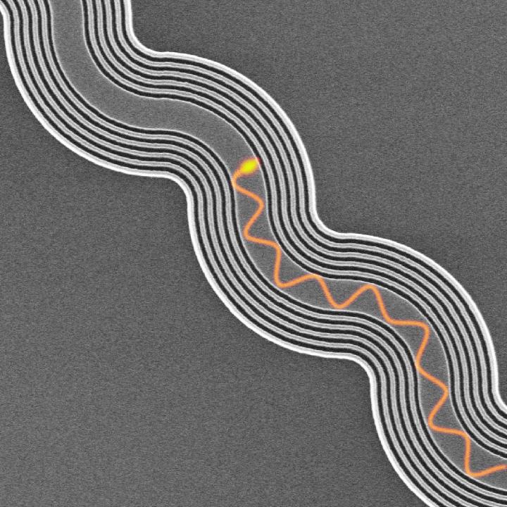
According to Purdue University, traditional computer chip components can undergo light-based replacements, which will increase the device’s speed thanks to light’s wide bandwidth.
Light-centered information processing has the potential to be more efficient than using the electrons of current devices. However, bit-carrying light streams have a tendency to leak out of the small, curvy highways on computer chips, called waveguides. This can lead to jumbled information, and decrease the integrity of communication.
A technique known as cladding is an important piece of the puzzle. It’s a protective metamaterial that helps stops light leakage as it travels through the computer chip. Overall, cladding can help support photonic integration within electric circuity, reduce power consumption, and increase communication speed.
Researchers from Purdue University have created unique waveguide cladding that targets the curviest travel sections.
“We want the bits of information that we are sending in the waveguide to travel along tight bends and simultaneously not be lost as heat. This is a challenge,” says Zubin Jacob, Purdue assistant professor of electrical and computer engineering.
Cladding allows light to travel different directions at different velocities, a characteristic referred to as anisotropy. The researchers were able to manipulate this feature, preventing light pathways from spilling into other streams. According to Purdue University, the bits instead bounce off by “total internal reflection” and stay within the confines of their waveguide.
“The waveguide we made is an extreme skin-depth structure, which means that any leakage that does happen will be really small. This approach can pave the way for dense photonic integration on a computer chip without worrying about light leakage,” says Saman Jahani, Purdue graduate research assistant in electrical and computer engineering.
The research paper, “Controlling evanescent waves using silicon photonic all-dielectric metamaterials for dense integration,” was published in the journal Nature Communications.
Below you can see an image of waveguide cladding.


