DC/DC conversion is the basic building block for many power converter designs including AC/DC power supplies, battery chargers, and uninterruptible power systems. This FAQ reviews some of the most common one-switch topologies. Specialty topologies such as the Joule Thief are not included. This article also does not consider various switched capacitor topologies, a review of those approaches can be found in “Switched capacitor power conversion for electronic systems.” The next FAQ will review two- and four-switch power conversion topologies.
Non-isolated single switch topologies
Buck Converter
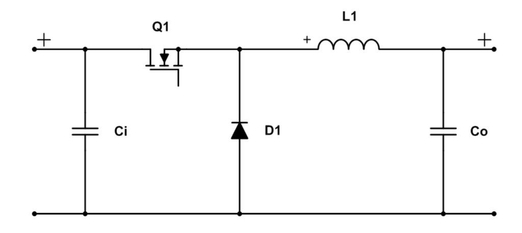
The buck converter is the most common power conversion topology (Figure 1). It steps down an input voltage to a lower output voltage. Among its many applications, the buck converter is widely used in distributed power systems to convert the bulk distribution voltage (usually 12 to 48 Vdc) to lower voltages such as 3.3V or 1.8V to power integrated circuits such as microprocessors, field programmable gate arrays, and so on. The inductor and rectifier are key elements in a buck converter. The current delivered to the load is the average value of the inductor current. To simplify output filtering, the inductor is usually specified so the output ripple is less than 30% of the load current. Replacing the rectifier diode with a FET for synchronous rectification results in a synchronous buck with significantly improved conversion efficiency.
Boost Converter
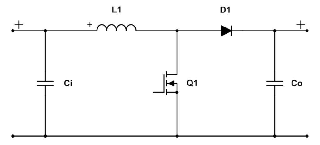
In a boost converter, the output voltage can be equal to or higher than the input voltage. (Figure 2). Increasing battery cell voltages is a common application for boost converters. To maintain stable operation, practical boost ratios are usually 3X or less. The input current increases proportionally with the boost gain. For example, a design that triples the input voltage also draws triple the input current. High pulsed input currents can result in electromagnetic interference (EMI) issues and lower conversion efficiencies. Because the input is connected directly to the output through the inductor and rectifier, turning off the PWM controller does not disconnect the input from the load. A second switch is needed to disconnect the input from the output.
Buck-Boost Converter
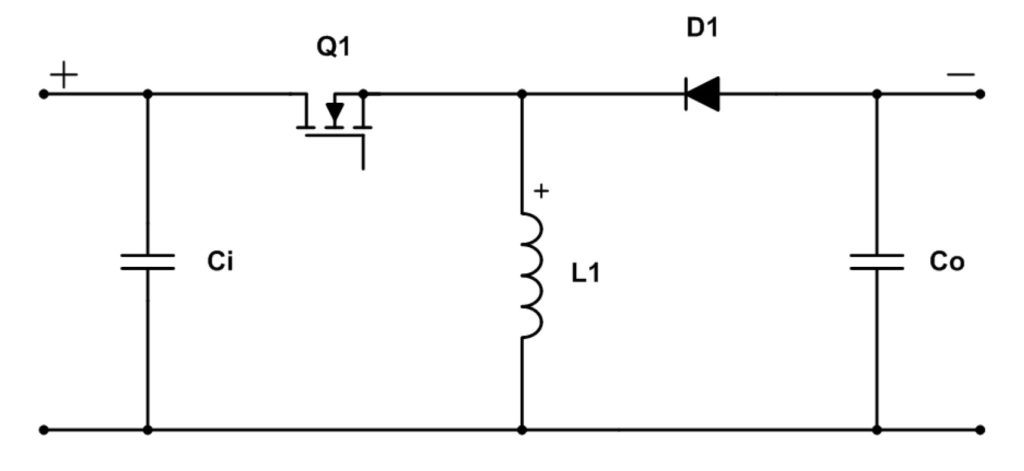
A basic, single-stage, buck-boost boost converter can supply a regulated DC output from a power source delivering a voltage either below or above the regulated output voltage. This topology is also called an inverting buck-boost since it converts a positive input voltage to a higher or lower negative output voltage level. Buck-boost converters are useful with variable voltage power sources such as photovoltaic cells or rechargeable batteries. In a synchronous buck-boost, the rectifier is replaced with a power MOSFET used as a synchronous rectifier.
Two-stage buck-boost topologies
The basic buck-boost topology described above includes a switch, diode, inductor and capacitor. A two-stage buck-boost converter includes a switch, diode, two inductors and two capacitors. The various arrangements of these elements can be used to produce several buck-boost topologies.
SEPIC
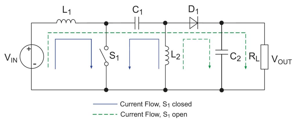
Like a basic buck-boost topology, a single-ended primary inductor converter (SEPIC) steps up/down an input voltage (Figure 4). Unlike a buck-boost, the output of a SEPIC converter is not inverted. SEPIC converters have a continuous input current which simplifies EMC challenges, but a pulsed output current and a complex feedback function making it challenging to maintain stable operation. Battery-powered systems and LED lighting are common applications for SEPIC converters. A SEPIC battery charger can recharge the battery and power the load at the same time.
Ćuk Converter
A Ćuk regulator converts a positive input voltage to a higher or lower negative output voltage level (Figure 5). The design of a Ćuk is similar to a SEPIC (two stages: boost converter followed by a buck converter), exceptiinductor L2 and diode D1 change places. Since the current flow is the same in both inductors, they can be wound on a single core as a coupled inductor, which reduces output ripple and increases efficiency. The transformer action between the coupled inductors results in lower output ripple compared with a Ćuk converter using two discrete inductors.
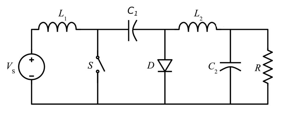
The continuous power transfer of a Ćuk converter minimizes EMI. This topology has continuous currents at both the input and the output, but the current stress on the switch is relatively high.
Zeta Converter
A Zeta converter is another variation on the SEPIC (Figure 6). Sometimes called an inverse SEPIC, the Zeta converter uses a buck converter followed by a boost stage, while the SEPIC has a boost stage followed by a buck. Like the SEPIC, the Zeta topology has a positive output voltage.
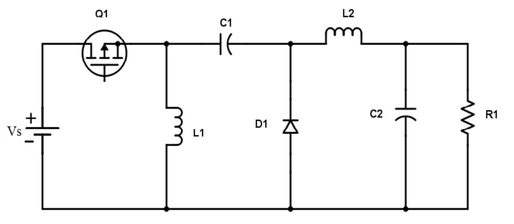
The feedback loop of a Zeta converter is more stable compared with a SEPIC and it can handle a wider input voltage range and higher output load transients. The output ripple of a Zeta converter is significantly lower than an equivalent SEPIC design. However, the Zeta topology suffers from a higher input ripple current, and requires a larger and more expensive coupling capacitor to support the same energy transfer as a SEPIC design.
Isolated one switch topologies
So far, all of the topologies have been non-isolated designs. It’s also possible to produce isolated converters with a single switch, including flyback and forward topologies. Forward and flyback converters can be used to either increase or decrease the input voltage, or convert a single voltage to multiple output voltages.
Flyback Converter
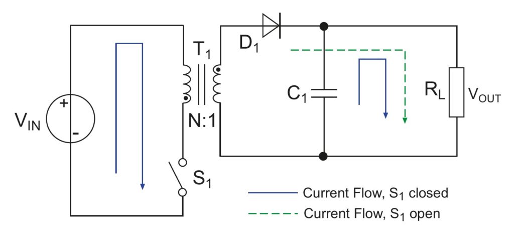
The Flyback topology is one of the lowest cost means generating power output up to about 150W, though some designs can support up to 250W (Figure 7). It can produce a higher or lower output voltage that can be positive or negative. A disadvantage is the high output ripple current. The “transformer” in a flyback converter is made up of two coupled inductors. This topology transfers energy to the secondary side only when the primary switch is off.
Figure 7: The “transformer” in a flyback converter is actually a pair of coupled inductors that store energy when the switch is on. Current flows to the output from the capacitor when the switch is on and from the stored energy in the transformer when the switch is off. (Image: RECOM)
The coupled inductor structure provides input-to-output isolation like a conventional transformer and is capable of supplying multiple isolated output voltages. It is possible to regulate the multiple output voltages with a single control. Flyback converters also operate over a relatively wide input voltage range and are used in a variety of applications include mobile device chargers, consumer electronics, standby power supplies and high-voltage power in cathode ray tubes (CRTs), lasers, copiers, xenon tubes and similar applications.
Forward Converter
A forward topology uses a true transformer (not the coupled inductors found in a flyback) to move energy from the primary to the secondary while the switching element is ON (Fugure 8). The transformer provides isolation and can be used to step the input voltage up or down and can provide multiple output voltages. The transformer in a forward converter includes a reset winding (connected to D3 in the figure below) to keep the transformer’s magnetic field from collapsing.
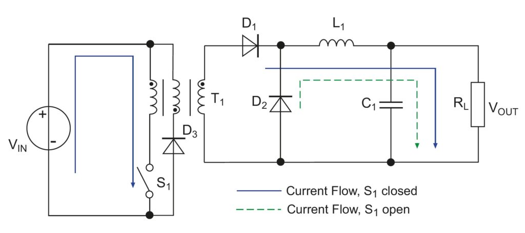
The output voltage of a forward converter is controlled by the input voltage, turns ratio between the primary and secondary transformer windings and the duty cycle. Forward converters are simple circuits with low current ripple on the input capacitor and the secondary diodes. But they require switching transistors rated for twice the input voltage and have a relatively large transformer as a result of the need for the reset winding. An active clamp circuit can be used to eliminate the need for the rest winding.
Active Clamp Converters
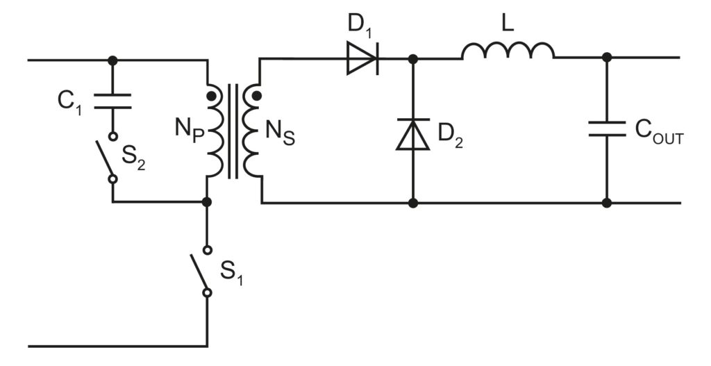
In addition to the basic components shown above, a flyback converter includes a resistor-capacitor-diode (RCD) clamp to reduce the voltage stress on the switching device. When the switch is turned OFF, voltage is reflected from the secondary side to the primary, stressing the switch. A passive primary-side RCD clamp can be added to protect the switch from potential damage, but at the cost of lower efficiency. An active clamp replaces the resistor in an RCD design with a switch. Instead of dissipating the leakage inductance energy, it recycles the energy back to the transformer. An active clamp can also be used to replace the reset winding on a forward converter, improving performance and simplifying the transformer design (Figure 9).
Summary
Single-switch dc/dc converter topologies are employed across a wide range of non-isolated and isolated power conversion applications up to a few hundred watts. The buck converter, which reduces the input voltage to a lower level, is probably the most-widely-used of all power conversion topologies. These topologies provide designers with an array of choices to optimize performance for specific application needs including EMI levels, efficiencies, delivery of single or multiple output voltages, and more.
References
Basic Concepts of Linear Regulator and Switching Mode Power Supplies, Analog Devices
Common Power Supply Topologies, XP Power
Comparison between Zeta Converter and Boost Converter using Sliding Mode Controller, International Journal of Engineering and Technical Research
Ćuk converter, Wikipedia
DC/DC Book of Knowledge, RECOM Power
Power Topologies Handbook, Texas Instruments

