Neither a Shockley diode nor a Schottky diode are single p-n junction devices. A Shockley diode has a four-layer thyristor structure with a typical forward drop of 800 mV. It’s called a diode because it has two leads. A Shockley diode is essentially a SCR with the gate not connected. In a Schottky diode a semiconductor and a metal such as molybdenum are bonded instead of a p-n junction to produce a forward voltage of 150 to 450 mV. This FAQ begins with a review of Shockley diode structure and operation, details the structure and operating specifications of Schottky diodes, and closes with a brief look at silicon carbide Schottky diodes.
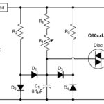
The Shockley diode—also called a PNPN diode, four-layer diode, or reverse-blocking diode thyristor—was one of the first semiconductor devices invented and was commercialized by the Shockley Semiconductor Laboratory in the late 1950s. A Shockley diode has a negative resistance characteristic and can be considered as a merger of two bipolar transistors, one NPN and one PNP, where the base of the top transistor is the same layer as the collector of the bottom transistor, and the base of the bottom transistor is the same layer as the collector of the top transistor (Figure 1). That structure results in the device’s unique operating characteristics.
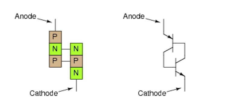
If a Shockley diode were an ideal device, neither transistor could turn on until the other transistor turned on since the base current through the upper transistor is controlled by the lower transistor, and the upper transistor controls the base current through the lower transistor. But Shockley diodes are not ideal devices, and when voltage is applied across the terminals, the transistors are not perfectly off, and each transistor conducts some leakage current. Once enough voltage (the breakdown voltage) is applied, the leakage current rises sufficiently, and one of the transistors turns on, allowing base current to flow through the other transistor, turning it on. The process is regenerative until both transistors are saturated and keep each other on.
Another way to turn on a Shockley diode is to force the device to latch using a fast-rising digital pulse. When the rise time of the pulse exceeds a specific threshold, the device will latch due to the junction capacitances between the various p-n junctions. If the rise time of the pulse is fast enough, the device will turn on, even if the signal level is not as high as that needed to turn on the device using a slower ramping voltage.
To turn a Shockley diode off, the voltage across the device needs to fall to a sufficiently low level so that the current flow is reduced below the holding current and is insufficient to maintain the transistor bias. One of the transistors will cut off, interrupting the base current to the other transistor and effectively turning the device off, returning it to a high impedance state.
The primary use of Shockley diodes was to control a silicon controlled rectifier (SCR). In fact, a SCR is the same structure as a Shockley diode, but with the addition of a gate connection to the p-type layer in the NPN transistor. If the gate of an SCR is not connected and left floating, the SCR can be used as a Shockley diode.
Schottky for fast switching and low Vf
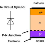
A Schottky diode–or more accurately a Schottky barrier diode (SBD)–is a structure in which a semiconductor and a metal such as molybdenum are bonded, in contrast with the p-n junction of a conventional diode. In general, commercial SBDs use an n-type semiconductor material and various metal junctions. Because they have a small forward voltage and a short “reverse recovery time,” SBDs are used in high-speed switching and rectification applications. Compared with a Shockley diode’s 800 mV forward drop and the 600 to 700 mV forward drop for a p-n diode, SBDs have typical forward voltages from 150 to 450 mV.
SBDs have a tradeoff between reverse current and forward voltage. Depending on the metal used, the breakdown voltage ranges from about 20 to 200 V. SBDs are available with a trench structure that improves their reverse current characteristics. Trench SBDs can offer a wider safe operating area. In addition, trench devices are often more robust relative to thermal runaway, making them preferred for higher temperature applications.
Strictly speaking, SBDs do not have a reverse recovery time. They are unipolar devices and do not experience carrier recombination like p-n diodes. However, the current flowing charges the capacity between the SBD terminals and appears similar to the reverse recovery of a p-n diode. As a result, it’s generally referred to as the reverse recovery time of the SBD.
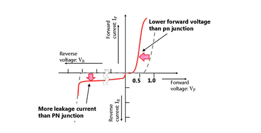
The I-V characteristics of an SBD differ from those of a p-n junction diode (Figure 2). Current rises exponentially in the forward direction, with a knee when the device turns on at about 0.2 V. Also, as seen in the I-V curve, SBDs have a lower forward voltage compared with p-n junction diodes. In the reverse direction, SBDs have a larger leakage current compared with p-n diodes.
SBDs used in small signal applications can benefit from the addition of a guard ring that improves the device performance in the forward and reverse directions. The main impact is a 4x improvement in breakdown voltage. Small signal SBDs without a guard ring may have a reverse breakdown of only 5 to 10 V, not enough for many applications.
SBD specifications
Some SBD specifications are quite different from those of p-n junction diodes, while others are only slightly different. In addition, there are different types of SBDs, for example, planar vs. trench and silicon vs. silicon carbide, with different performance characteristics. And the “same” SBDs sourced from different manufacturers may not be identical. It’s therefore important to have an understanding of basic SBD specifications:
Forward voltage drop
The forward voltage drop is a key specification and varies according to the current being carried. It’s typically specified for a given current. Relatively low forward voltage drops are an advantage of SBDs.
Reverse breakdown
Not only is the forward voltage drop lower for SBDs, but so is the typical breakdown voltage compared with standard p-n junction diodes. There can be several parameters related to reverse breakdown, such as maximum peak reverse voltage, maximum repetitive reverse voltage, maximum blocking dc voltage, and so on. If any of these parameters is exceeded, the device can be damaged.
Capacitance
Capacitance is particularly important for small signal RF design applications; even small values of capacitance can have a significant impact on circuit performance. The junction areas of SBDs are small, and therefore the capacitance is small, often just a few picofarads. Capacitance is specified at a given voltage.
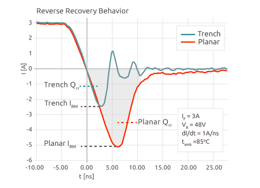
Trench SBDs have higher parasitic capacitance compared with planar devices. However, due to their higher current density, trench SBDs have a smaller effective junction capacitance compared to planar SBDs. As a result, trench SBDs have much less stored charges (Qrr) and are preferred for high-frequency rectification applications (Figure 3).
Reverse recovery time
Reverse recovery, the time it takes to transition from a fully ‘on’ to a fully ‘off’ state, is particularly important in switching applications. The current that flows during this time period is the ‘reverse recovery charge.’ This specification for SBDs is measured in nanoseconds or picoseconds. In an SBD, reverse recovery time arises from the capacitance rather than from the majority carrier recombination that takes place in a p-n diode. There is very little reverse recovery overshoot with SBDs.
Reverse leakage current
Reverse leakage current is an important specification. It increases significantly at elevated operating temperatures. It can increase by an order of magnitude for a given level of reverse bias for every 25 °C increase in the junction temperature. Trench SBDs can have better reverse leakage characteristics compared with planar SBDs.
Working temperature
The maximum working temperature of the SBD junction is usually between 125 to 175 °C. This is less than the 200 °C specification for many p-n junction diodes. This can be particularly challenging when the SBD is used as a power rectifier. If the maximum working temperature is exceeded, device reliability will be reduced.
SiC Schottkys
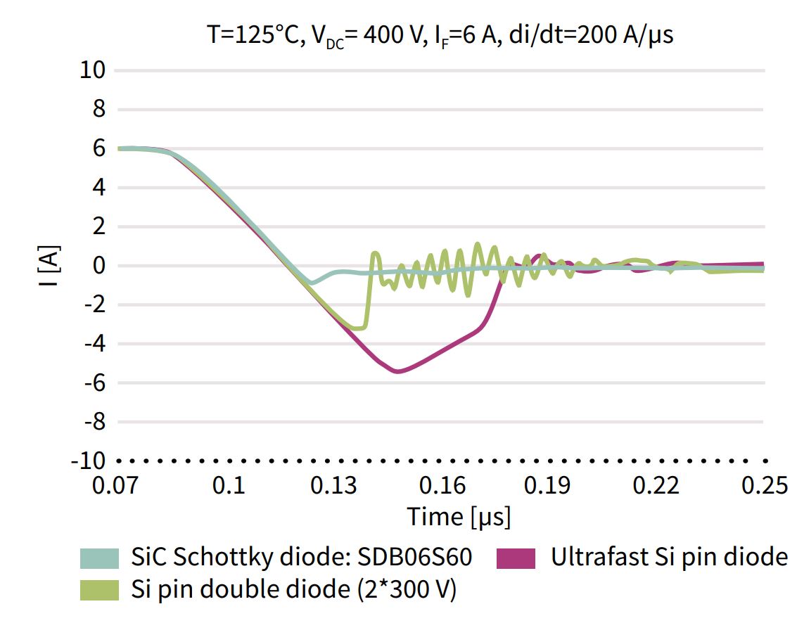
The use of SiC brings well-known benefits to SBDs. Compared with Si devices, SiC SBDs have better electrical and thermal conductivity. That makes it possible for SiC SBDs to deliver a low forward voltage drop across the entire operating temperature range of the diode. The majority carrier characteristics of SiC SBDs result in no reverse recovery charge, and the only contribution to the switching losses comes from the tiny capacitive displacement charge. In the same voltage range, silicon SBDs have much higher switching losses (Figure 4). These characteristics contribute to higher efficiency power conversion, smaller heat sinks, and lower electromagnetic interference (EMI) when using SiC SBDs.
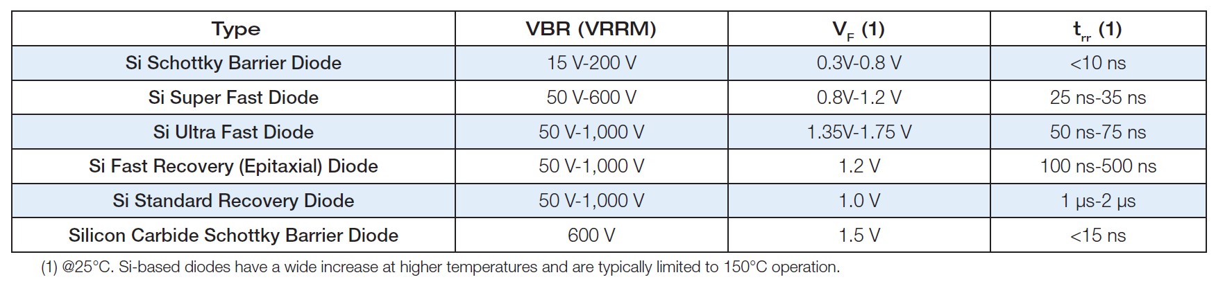
Of course, it is not as simple as a choice between Si and SiC, there’s a wide variety of diode implementations available with a range of tradeoffs related to VF and trr, as well as other specifications (Table 1). While SiC SBDs continue to gain market share, other rectifier types continue to be used in specific application areas.
Summary
Shockley and Schottky diodes are quite different devices. While Shockley devices are based on a thyristor structure and were one of the earliest semiconductor devices to be commercialized, SBDs, especially SiC SBDs, represent the latest developments in diode and rectifier technology. With the growing variety of SBDs available, designers need to have a clear understanding of the features and benefits of Si and SiC devices, plus the growing variety of device structures that are available.
References
CoolSiC Schottky Diodes, Infineon
Schottky Barrier Diodes, Toshiba Electronic Devices & Storage
Silicon Carbide Schottky Barrier Diodes, Rohm
The Fundamentals of Silicon Carbide Schottky Diodes, Wolfspeed
The Shockley Diode, IDC
Why Trench Schottky rectifiers are the preferred choice, Nexperia