
By Allan Saliva Lead Principal Application Engineer, Infineon Technologies
Power supply engineers have been designing power supplies using silicon transistors for years. Now they are asking, what are the application benefits of using GaN and how do you use it to enable the highest level of performance at a reasonable cost? This article provides technical guidance for system designers transitioning from Silicon to GaN-based architecture. It outlines the fundamental performance differences between GaN and Silicon (Si) and explores how these differences affect circuit behavior.
Over the past 30 years, power supplies have experienced dramatic improvements in efficiency and power density. One of the key drivers for improving power supply performance is the advances in power semiconductors technologies such as trench MOSFETs, superjunction FETs, and Silicon Carbide (SiC) Schottky diodes. All of this happened while the cost per watt reduced significantly.
Facing power supply efficiency certification such as 80 PLUS Titanium (96% efficiency at 50% load) designers need to take advantage of the performance improvements that GaN provides. GaN’s low on-resistance (RDSon), low gate charge (Qg), low output charge (Qoss), and no reverse recovery charge (Qrr) help maximize efficiency and power density of the power supply. However, GaN is not a simple drop-in replacement for Silicon MOSFETs due to its distinctive characteristics.
Let us consider a simple boost CCM PFC (Critically Conduction Mode Power Factor Correction) converter as shown in Figure 1 and examine where the losses are coming from. Input diode bridge rectifies the AC input voltage. In the boost converter, when the main switch Q1 is turned on, inductor current ramps up through L1 and then steers to the bus capacitor when Q1 is turned off.
The high frequency switching (typically ~100kHz) of the boost converter causes switching losses on Q1. However, the majority of the losses are in input bridge reciter conduction, which accounts for around one third of the total power loss.

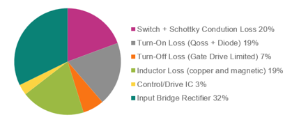
Figure 1. CCM PFC (a) Circuit Schematic (b) PFC Power loss summary Po=400W, Vin=90Vac. (Image: Infineon)
Figure 1b shows the power loss distribution for a typical boost converter at 400W output (400V/1A) and 90Vac input voltage. Based on this graph, even if we replace Q1 with an ideal switch to get rid of all the switching losses, it will not make a significant difference compared to getting rid of the bridge rectifier loss. We need to look for a topology to get rid of a bridge rectifier and take advantage of GaN capabilities.
One way to do it is to replace the rectifier diodes with MOSFETs, that is using bridgeless rectifiers, to reduce conduction loss. However, it would require four large FETs and floating gate drivers, which increases design complexity and cost.
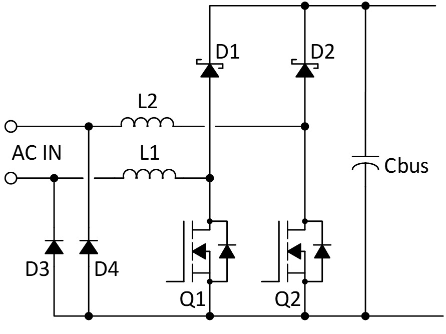

Figure 2. Dual Boost Topology (a) Partial bridgeless (b) Fully bridgeless. (Image: Infineon)
A topology called dual boost PFC is another way to minimize bridge rectifier losses. It uses two active boost converter sections. One section operates during the positive half of the AC line cycle, and the other operates during the negative half-cycle. A partial bridgeless dual boost topology (Figure 2a) uses only two input rectifiers instead of four.
Eliminating the input rectifier is possible by replacing the two rectifiers with MOSFETs (Figure 2b). For the boost diodes D1 and D2, it is important that they do not have reverse recovery (or very minimal) characteristics so a SiC diode is the choice for best efficiency. This topology can achieve up to ~98% efficiency, however, it uses 4 big MOSFETs, 2 inductors and 2 SiC diodes.
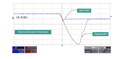
Let us step back and take a closer look at the reverse recovery characteristic of a boost diode used in CCM PFC, as shown in Figure 3. If D1 is a Silicon diode, which is a minority-carrier device, it will have excess-carrier Qrr. Reverse recovery loss in a boost converter occurs when the boost diode (or synchronous MOSFET) switches from a conducting state to a blocking state, allowing a transient reverse current to flow. This transient current creates a significant power loss which is proportional to the reverse recovery charge of the device (Qrr) and switching frequency. Choosing a device with high reverse recovery characteristics not only affects overall efficiency, but it also causes voltage ringing and high current spikes. Figure 4 shows waveforms comparing reverse recovery performance of a GaN vs Si superjunction MOSFET to show the huge Qrr difference. This should make it clear why superjunction simply would not work for hard-switched CCM PFC – the losses due to Qrr would be HUGE. If we could replace the boost diode and MOSFET with GaN, we will see significant improvements in efficiency.
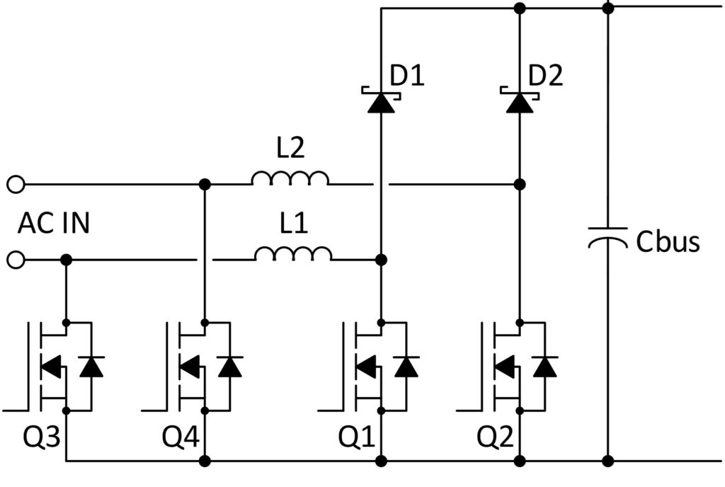
A bridgeless totem-pole PFC (Figure 4) is a pair of half-bridges, one operating as a low-frequency synchronous rectifier (slow switching leg, Q3 & Q4) and the other as a high-frequency synchronous boost rectifier (fast leg, Q1 & Q2). This is a simple topology with no diodes, eliminating the conduction losses associated with diode’s forward voltage drop. The use of GaN in the high frequency leg minimizes switching losses. There is no reverse recovery loss during hard switch turn on, and turn off loss is close to zero. Note that for CCM operation Q1 and Q2 cannot be MOSFETs due to large Qrr. Slow switching leg Q3 and Q4 can be low RDSon low-cost MOSFETs. This topology combining GaN with Silicon can achieve peak efficiency (greater than ~99% at 230Vac) as shown in Figure 4b; measured on a 2.5kW Totem pole PFC GaN evaluation board at 230Vac input voltage.
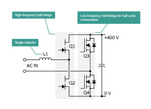
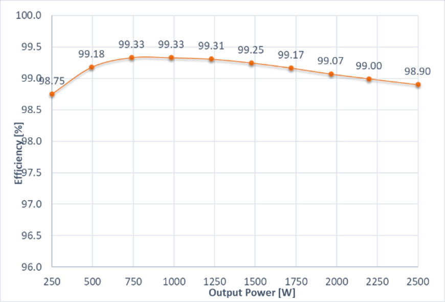
Figure 5. Bridgeless “totem pole” PFC (a) basic schematic (b) efficiency. (Image: Infineon)
Let us now look at the DC-DC stage to see how we can use GaN to get similar improvement in performance. The LLC resonant converter is a widely used, high-efficiency topology for power supplies in the range of 100W -1kW+. It is a resonant converter topology composed of a half or full bridge switch, transformer, and resonant tank. Lossless switching enables high efficiency design of around 98%, even with MOSFET switching at ~100kHz-150kHz.
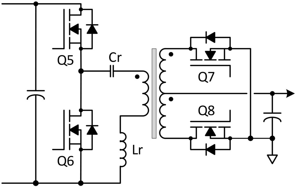
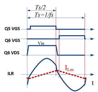
Figure 6. LLC converter (a) basic schematic (b) waveforms. (Image: Infineon)
To achieve ZVS (Zero voltage switching) of the half bridge switch, the magnetizing inductance energy is important to discharge the Coss of the half bridge node during the dead time interval. We can see this in the waveforms where magnetizing current should be sufficient to fully discharge the parasitic output capacitance ( Qoss) of the primary-side MOSFETs during dead time. The peak magnetizing current is directly proportional to Qoss and inversely proportional to dead time (ILmag_pk=2*Qoss/dead time).
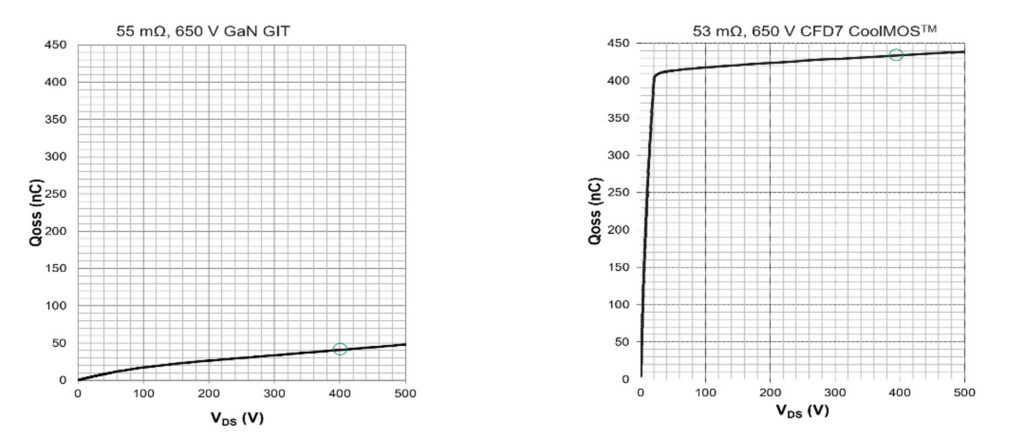
Comparing Qoss of GaN and Superjuntion MOSFETs, we can see that GaN has ten times lower Qoss than MOSFET (40nC vs 430nC at 400Vdc). Exceptionally low charge is one of the key benefits of GaN to enable higher frequency operation without increased losses.
To understand it better we must look at the dead time and peak magnetizing current as the frequency increases. At 150kHz the dead time is ~350ns (5% of the period) and we could get reasonable peak magnetizing current using MOSFET. However, if we want to operate at 800kHz, dead time decreases significantly to 60ns; if we use the same Silicon Qoss, the magnetizing current needs to increase six times. This will result in larger RMS current and i2R conduction losses will increase thirty-six times. Using GaN with ten times lower Qoss could reduce the magnetizing current by 40%.
Let us now look at the secondary side synchronous rectifiers. The output current of the LLC converter has high ripple and high RMS current. Often, we parallel SR switch to lower conduction loss and improve thermal management. Silicon MOSFETs at this lower voltage range have particularly good RDSon and high current rating, but also have high gate charge. Driving multiple devices in parallel at high frequency is a major burden for the gate-drive circuit. Typical gate-charge of GaN vs Si low-voltage FET with the same Rds(on) is ten times lower for GaN. Once again, the low charge of GaN is a significant benefit compared to Silicon–even on the low voltage side.
Today, using GaN enables the highest levels of performance at a reasonable cost. The incredibly low gate charges (Qg, Qoss) and zero reverse recover characteristics (Qrr) are key attributes that allow GaN to have the lowest switching losses in any transistor technology for high voltage applications, regardless of switching frequency. For medium voltage, such as synchronous rectification, GaN is easier to parallel from a single gate driver. As GaN production scales up, it will reach price parity with Silicon and GaN will become default choice for any power applications.