
by Volker Brichzin, Senior Director Engineering, TE Connectivity
It’s all about plating
Modern design engineers face a conflicting mandate: systems require unprecedented signal integrity and mechanical durability, yet corporate directives demand a reduction in both production costs and product carbon footprints (PCF). At the center of this challenge is the connector interface. One decisive factor for the electrical and mechanical performance of a connector system is the surface finish of the contacts.
A connector must perform effectively during operation and withstand high loads. The contacts are particularly crucial, as they must support excellent electrical conductivity to ensure reliable signal and power transmission. Consequently, it is paramount to meet both electrical and mechanical requirements when selecting plating materials applied on the contact base material. Well-chosen plating materials enable low contact resistance to minimize losses. Additionally, the chosen materials protect the contact zone from corrosion and provide reliability with regards to mating cycles and micro movement.
Plating protects against corrosion
The surfaces of a connector rely on the number of microcontact points — the higher the number between two surfaces, the more reliable the transmission performance. When corrosion occurs, these microcontact points are reduced and performance degrades. In high-vibration applications like automotive or industrial machinery, mechanical stress induces micro-movements at the contact interface. This leads to fretting corrosion, where traditional soft gold or crystalline structures wear away, exposing the base metal to oxidation and sulfur reactions that generate non-conductive layers. This is why optimizing surface treatments is paramount.
In the past, good results have been achieved with plating made of precious metals, especially gold. Since the costs of these feedstocks can fluctuate heavily and have an adverse impact on the product carbon footprint (PCF), it is important to make the metal layer as thin as possible. Due to technical reasons (e.g., electroplating process capability), there is a limit to the layer thickness for metal plating and a need for an additional underlayer to optimize the whole plating performance. This “barrier layer” made of nickel is intended to prevent atoms on the contact surface from diffusing into the base material. The contact layer is placed on top of this barrier and has the main task of protecting against corrosion and providing a low friction coefficient. It can be made of full gold or palladium-nickel with gold flash.
Even the gold standard has disadvantages
Gold surfaces on a nickel barrier layer have proven themselves when it comes to supporting high-performing features, such as a high number of mating cycles. The unique material properties of gold make it extremely resistant to oxidation, which prevents corrosion and wear. Gold-plated contacts were considered the premium solution. There are also some disadvantages, such as cost fluctuation and an unfavorable carbon footprint. As a result, efforts are being made to reduce the gold layer.
TE Connectivity (TE) has conducted intensive research to optimize the plating technology for connector contacts with a goal of matching the plating layers (including the barrier layer) in a sophisticated stack configuration so that effective results can be achieved even in demanding applications while taking environmental requirements into account.
The science behind amorphous alloys
The use of nickel phosphor is established in industries like printed circuit board manufacturing, but its historical application via chemical processes was too costly for mass-market connector production. Through advanced electroplating, this alloy can now be applied in a highly controlled process to ensure that the phosphor content remains above 11.5%. At this threshold, the alloy transitions from a crystalline structure to an amorphous, glass-like state.
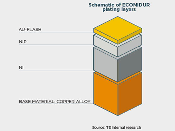
Unlike pure gold — which is naturally soft — or traditional hard gold alloys containing small amounts of cobalt or nickel, this amorphous structure provides exceptional hardness and superior abrasion resistance. It acts as an ultra-hard protective barrier over the underlying copper, shielding it from oxidation and sulfur reactions that generate non-conductive surface layers, as shown in Figure 1.
Extending lifetime under harsh conditions
Rigorous testing-to-failure reveals that this nickel phosphor formulation outperforms traditional benchmarks like palladium-nickel. In comparative wear evaluations depicted in Figure 2, the contact resistance of the nickel phosphor plating remains remarkably stable, showing a nearly flat baseline noise level until the very end of testing. This translates to an operational lifetime three to four times longer than that of palladium-nickel.
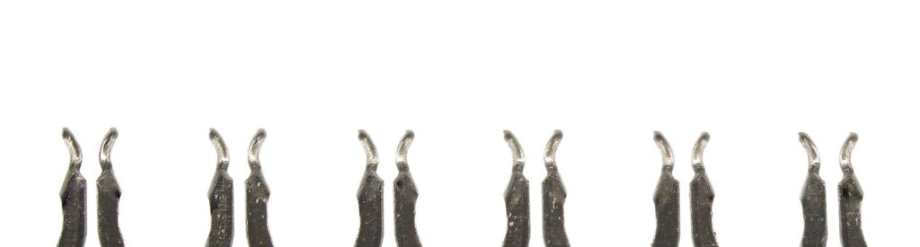
Such durability is highly advantageous for applications subjected to extreme vibration and high mechanical loads, where standard connectors would typically fail or require frequent maintenance. Furthermore, the material maintains excellent signal integrity up to the 32 Gbps range due to its electromagnetic permeability of 1.
A sustainable and cost-effective roadmap
Beyond mechanical superiority, the shift to nickel phosphor addresses urgent environmental and economic demands. Plating layers are the primary drivers of carbon emissions in board connectors. Standard precious metals like gold and palladium are highly energy-intensive to mine and refine, resulting in severe product carbon footprints.
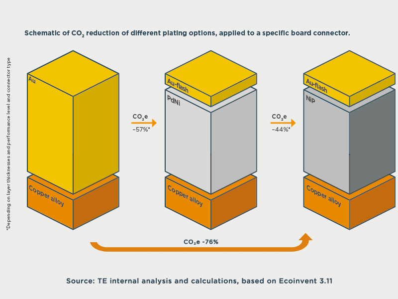
Using data from the Ecoinvent life cycle inventory database, lifecycle calculations confirm that replacing or minimizing these materials yields quantifiable sustainability benefits. For instance, by utilizing an ultra-hard underlayer, the traditional one-micron gold standard can be reduced to a mere “flash” layer of 0.1 microns — just 15% of the traditional one-micron standard. As Figure 3 illustrates, this approach maintains critical mating properties while slashing the product’s overall carbon footprint, allowing engineering teams to meet strict corporate ESG metrics without sacrificing reliability.
Economically, this transition offers substantial cost savings compared to thick gold and is motivation for original equipment manufacturers to initiate qualification testing. Because the industrial and automotive sectors operate on conservative platform lifecycles of 10 to 15 years, component engineers are understandably hesitant to alter qualified bills of materials. Integrating this technology during the design phase of new platforms mitigates risk early. Embracing these advanced plating stacks now helps ensure that manufacturers don’t miss the window of opportunity to build future- ready, cost-stable, robust, and sustainable systems.