
Differential pairs in high-speed serial links require tight control of impedance, skew, and coupling to limit reflections, mode conversion, and crosstalk. At multi-gigabit data rates, small deviations in trace geometry, routing symmetry, or material properties degrade eye diagrams and result in protocol non-compliance.
This article reviews the primary signal integrity requirements for differential pairs in high-speed serial interfaces: differential impedance control, skew management, crosstalk reduction, and PCB layout techniques that maintain signal quality from driver to receiver.
Differential impedance control
Differential impedance is the primary electrical parameter determining signal transmission in a routed differential pair. It equals twice the odd-mode impedance of each trace and depends on width, intra-pair spacing, copper thickness, dielectric height, and dielectric constant. Common serial interfaces target 85–100 Ω: PCIe Gen 4/5 specifies 85 Ω, USB 3.2 and USB4 target 90 Ω, and LVDS typically specifies 100 Ω.
As shown in Figure 1, differential impedance depends on trace width, spacing, and dielectric geometry across both microstrip and stripline configurations.
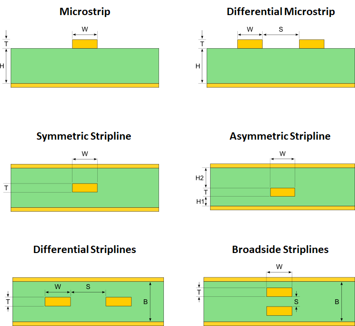
Maintaining target impedance requires a controlled stackup. Trace geometry is tied to a field solver or fabricator impedance table, with width and spacing held constant along the full length of the pair.
Discontinuities such as neck-downs, anti-pads, asymmetric via structures, and unsymmetric component pads introduce local impedance perturbations that generate reflections and degrade the eye opening. Small passive packages, typically 0402 or smaller for AC-coupling capacitors, and symmetric placement on both legs reduce component-induced asymmetry.
A solid, unbroken reference plane beneath or around the pair is equally critical. Microstrip pairs route over a continuous ground plane, while stripline pairs route between ground or power planes. Plane splits, voids, or gaps beneath the pair raise local impedance and increase radiated fields. Controlled-impedance requirements, typically ±10%, should appear in fabrication notes and be enforced as net-specific constraints in the PCB tool.
Closed-form equations such as IPC-2141 provide approximate results and lose accuracy for many geometries at higher frequencies. Field-solver-based tools, including calculators such as Polar SI9000, provide more reliable starting geometries. For critical links, the S-parameter or TDR simulation verifies the realized impedance before fabrication.
Skew management
Skew is the propagation delay difference between the P and N legs of a differential pair. It converts differential energy into common-mode noise, degrading the eye opening and increasing electromagnetic emissions. At multi-gigabit data rates, intra-pair skew budgets are tight. PCIe Gen 5 allows a few tens of picoseconds, which can translate to length matching on the order of a few mils on standard FR-4.
The most common source of skew is asymmetric routing. As shown in Figure 2, skew results from unequal path lengths between differential pair legs and is corrected using distributed serpentine tuning while avoiding localized discontinuities.
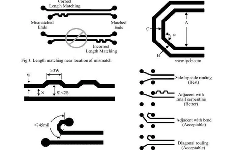
Keeping both legs geometrically symmetric, with identical bend count, matched via structures, and parallel paths over the same reference planes, eliminates most routing-induced delay mismatch.
When length tuning is required, serpentine segments on the shorter leg restore timing alignment. Distributed tuning over a longer routing section produces better results than compact serpentines placed near a connector or receiver, which introduce localized capacitive loading and crosstalk.
Other contributors include via structures and material effects. Each via adds capacitive loading and, if not back-drilled, leaves a stub that resonates at frequencies inversely proportional to stub length. Matched via placement on both legs, along with back-drilling in high-speed designs, keeps via-induced skew within budget.
Material properties introduce a less obvious but significant skew mechanism. Glass-weave variation in standard FR-4 laminates can add 10–100 ps of skew at 10 Gbps and above, even when trace lengths are matched. One leg may route predominantly over glass bundles while the other routes over resin pockets, producing different effective dielectric constants and propagation velocities.
Low-Dk, low-variation laminates, slight trace angle offsets relative to the weave direction, or weave-skew-aware materials reduce this effect in demanding designs. Skew matching should account for the full signal path, including package traces, connector pins, and via delays, rather than PCB trace length alone.
Crosstalk reduction
Differential signaling rejects common-mode noise, improving immunity to external aggressors. Parallel high-speed pairs can still couple into each other and into adjacent single-ended nets when spacing and referencing are inadequate.
As shown in Figure 3, crosstalk originates from electromagnetic coupling between adjacent conductors, increasing with reduced spacing and longer parallel routing length.
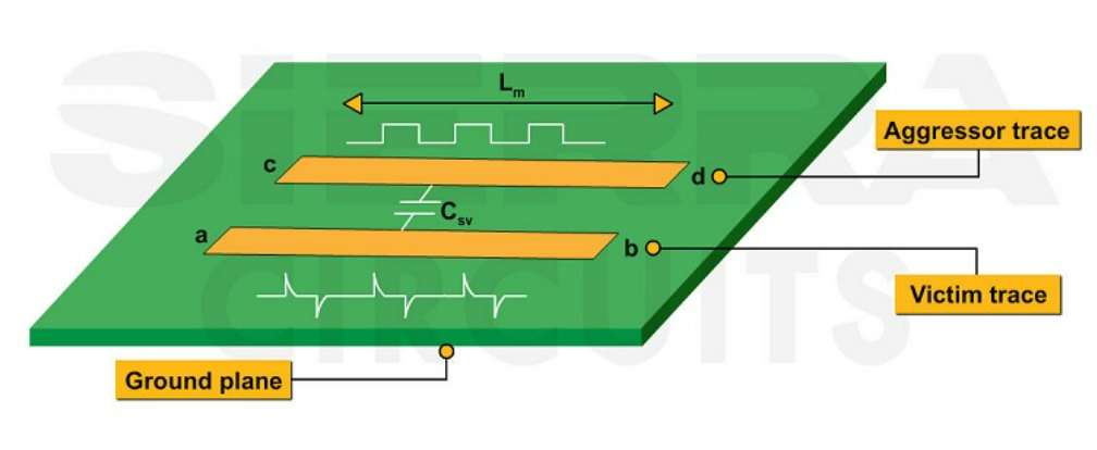
Tight intra-pair coupling, defined by a small spacing between the P and N legs, reduces loop area and radiated fields, improving common-mode rejection. Inter-pair spacing controls crosstalk between adjacent differential pairs.
A common guideline specifies edge-to-edge spacing of three times the trace width, or approximately five times the intra-pair spacing. This keeps differential crosstalk within acceptable limits for most multi-gigabit interfaces. Closer proximity to a reference plane reduces the required inter-pair spacing for a given crosstalk target, which is one reason stripline routing provides better crosstalk performance than microstrip at equivalent pitch.
Physical separation between aggressor nets and sensitive differential channels is also critical. Clock traces, DDR buses, and fast-switching power nets should not run parallel to PCIe, USB, or LVDS pairs over extended distances. Long parallel runs increase coupled energy in proportion to the coupled length, regardless of spacing. Routing strategies that minimize parallel overlap, combined with layer assignments that place sensitive pairs away from noisy nets, are more effective than spacing adjustments alone.
PCB layout techniques for high-speed serial interfaces
High-speed serial interfaces such as PCIe Gen 4/5, USB4, and LVDS require consistent, symmetric routing with minimal discontinuities. Effective layout begins at the routing channel level. Each pair should run as straight as possible with minimal layer changes. When layer changes are required, both legs transition together using matched via structures on the same footprint.
Maintaining constant spacing and width across the pair, including through bends, preserves differential impedance. Shallow 45-degree bends or arc-based routing reduce impedance perturbation compared with 90-degree turns. AC-coupling capacitors, electrostatic discharge (ESD) protection devices, and connector pads should be placed symmetrically on both legs, with stub lengths kept as short as possible.
As shown in Figure 4, asymmetric component placement introduces imbalance between differential pair legs, while symmetric placement maintains signal integrity.
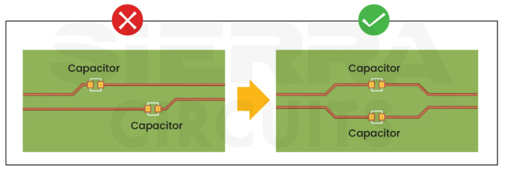
Component-induced asymmetry is a common source of mode conversion that impedance control alone cannot correct.
Constraint-driven routing enforces these requirements. PCB design tools allow net-specific rules for differential impedance, intra-pair spacing, length, skew tolerance, and via usage. Defining these constraints before routing begins prevents manual edits or autorouter decisions from breaking pair symmetry. For PCIe Gen 5 and USB4 designs operating at 32 GT/s and 40 Gbps, SI simulation using extracted S-parameters and eye diagram analysis should validate the channel before fabrication.
Mechanical design also affects signal integrity. Securing hardware such as standoffs and jackscrews near connector locations rather than at board corners reduces PCB flexure and solder-joint stress during assembly and thermal cycling.
Connectors positioned close to the board’s rigid attachment points experience less thermally induced displacement, which is relevant in differential connector systems where contact geometry affects impedance and insertion loss.
Summary
Signal integrity in high-speed serial link differential pair designs depends on coordinated control of impedance, timing, coupling, and layout geometry. Differential impedance is set by stackup and trace geometry and must remain constant along the routed length, with field-solver-based verification for demanding interfaces such as PCIe Gen 5 and USB4.
Skew management requires symmetric routing, distributed length tuning, matched via structures, and attention to glass-weave variation at higher data rates. Crosstalk control relies on tight intra-pair coupling, adequate inter-pair spacing, and separation from high-aggressor nets.
These requirements extend to layout discipline, including symmetric component placement, minimal discontinuities, constraint-driven routing, and SI simulation, ensuring consistent signal integrity from driver to receiver.
References
A Signal Integrity Guide to HSD PCB Design, Cadence
Differential Pairs: From Basic Concepts to Advanced PCB Routing, Cadence
10 Best High-Speed PCB Routing Practices, ProtoExpress
Why Controlled Impedance Really Matters, ProtoExpress
A Beginners Guide to Impedance Control in PCBs,
JLCPCBDifferential Pair Routing Guidelines for High-Speed PCB Design, PCBWay
3 Methods for Routing High-Speed PCB Designs, Zuken
Signal Integrity Analysis, Zuken
LVDS PCB Layout Guidelines for Ensuring Signal Integrity, Altium
PCB Impedance Simulation: Tools and Techniques for Accurate Design, AllPCB
How Dielectric Constant Affects PCB, Stanford Advanced Material
Controlled Dielectric or Controlled Impedance, PCB Prime
Material-Induced Skew in High-Speed Multilayer PCBs: Influences and Mitigation Strategies, Signal Integrity Journal
Related EEWorld Online content
What is Gate Charge, and Why Does it Matter for Switching Speed?
Why do High frequency Signals Reflect?
Avoid Ground Loops in Mixed-Signal Circuits Part 1
Avoid Ground Loops in Mixed-Signal Circuits, Part 2
When Are Signal Conditioners Not Needed With Sensors?