
By Todd Burkholder, Sudarshan Deo, and Muhammad Hassan, Siemens EDA
The relentless pursuit of artificial intelligence (AI) innovation has ushered in an era of unprecedented computational demand, pushing the boundaries of traditional silicon architecture. As Moore’s Law decelerates, the industry faces a critical juncture where conventional 2D monolithic designs can no longer meet the escalating requirements for bandwidth, latency, and power efficiency demanded by next-generation AI workloads. In response, 3D IC technology has emerged as a pivotal enabler, offering a pathway to overcome these scaling bottlenecks and unlock new levels of performance. However, this new architectural approach introduces profound design complexities that necessitate a revolutionary approach to EDA, one deeply rooted in industrial-grade AI.
The increasing sophistication of AI, particularly in transformer-based models, underscores a fundamental shift in chip design philosophy. Instead of merely adapting software to existing hardware, the focus has moved to architecting silicon specifically for AI workloads. This “AI-first chip design” paradigm mandates hardware capable of massive parallelism and high-speed data movement, all while adhering to stringent power and thermal limits.
3D IC technology directly addresses these critical demands through the vertical integration of multiple dies, such as High Bandwidth Memory (HBM) with logic, utilizing through-silicon vias (TSVs). This vertical stacking dramatically elevates bandwidth, with HBM4 stacks now delivering up to 3 TB/s per stack, and significantly reduces latency. Such advances are indispensable for the development of advanced AI accelerators and high-performance computing systems.
3D IC design considerations
While 3D IC innovations offer substantial performance gains, they simultaneously introduce design complexity at the system level. Here are four of the more critical challenges.
Power and Thermal Management: AI chips are inherently power-intensive. The dense stacking characteristic of 3D ICs exacerbates heat dissipation issues, demanding sophisticated cooling solutions and precise thermal-power co-analysis to avert thermal runaway and performance degradation. HBMs, in particular, are sensitive to temperature fluctuations, making temperature balancing a formidable task given their proximity to high-power computing dies.
Chiplet-to-Chiplet Interconnectivity: The integration of HBM and heterogeneous chiplets relies on advanced 3D stacking and nanometer-scale interconnect technologies, including micro-bumps, hybrid bonding, and TSVs. At these minute scales, even marginal defects, such as increased contact resistance, misalignment, or voids, can compromise signal integrity, disrupt power delivery, and impair system functionality or long-term reliability. Beyond physical integration, die-to-die connectivity presents significant hurdles in ensuring robust high-speed communication across chiplet boundaries. Interfaces operating at tens of gigabits per second must maintain tight design margins while traversing complex package structures like interposers or embedded bridges.
System Integration Complexity: Modern AI chips can contain billions of transistors. Designing these intricate 3D ICs, with their multi-chiplet planning, inter-die connectivity, and system-level modeling, pushes traditional EDA tools beyond their manual capabilities. Unlike monolithic SoCs, 3D IC architectures introduce tightly coupled interactions across dies, interposers, and packages. Early decisions in system partitioning—such as chiplet granularity, floorplanning, and interface selection—directly influence signal integrity (SI), power integrity (PI), latency, and overall system performance. Consequently, system integration for 3D ICs necessitates a shift towards unified, system-driven design methodologies.
Scalability: The adoption of chiplet-based architectures and 2.5D/3D-IC stacking, while promoting modularity and scalability, complicates “what if” scenarios for signal timing and vertical power delivery. Even minor alterations in floorplanning or chiplet placement can have cascading effects across the system, impacting timing margins and overall throughput. Traditional design methodologies, heavily reliant on human intuition and iterative refinement, are ill-equipped to efficiently navigate this expanding design space. What was once a manageable set of tradeoffs in 2D SoC design transforms into a high-dimensional optimization problem in 3D IC systems.
These challenges underscore the critical need for a new class of EDA methodologies that transcend conventional flows, leveraging machine learning (ML), reinforcement learning (RL), generative AI, and agentic AI to scale design expertise and accelerate the design, simulation, and validation of complex 3D IC architectures. These new AI-driven methodologies enable automation and optimization across the design flow, tackling the immense complexity that human engineers can no longer manage alone. The rest of this article summarizes key trends where 3D IC and AI interweave.
AI-driven imperatives for 3D IC design
AI is fundamentally transforming EDA by embedding ML and RL techniques directly into design tools. EDA vendors, such as Siemens, are integrating these capabilities within a unified, system-driven workflow for 3D ICs. This approach enables automation and optimization across the design flow, effectively tackling the immense complexity that human engineers can no longer manage alone. As a result, AI not only enhances productivity but also fosters more predictable performance and reliability in next-generation AI and high-performance computing (HPC) systems.
Intelligent Design Space Exploration (DSE)
3D-IC architectures are exponentially complex, requiring designers to balance thousands or millions of interdependent variables (die partitioning, material stacks, floor planning, interconnect topology, and power delivery), while optimizing for power, performance, and area (PPA), reliability, and cost. Manual iteration is slow and prone to suboptimal outcomes.
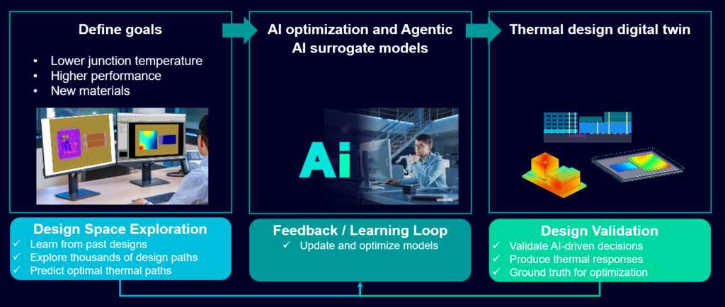
AI, through ML, RL, and surrogate modeling, drastically accelerates intelligent design space exploration (DSE). It allows teams to predict outcomes faster. AI models can quickly evaluate the impact of design choices. AI can learn from previous iterations. Knowledge gained from past designs can be applied to new projects, reducing ramp-up time for next-generation architectures. It can be used to uncover unconventional architectures. AI can identify optimal architectural plans that might be overlooked by traditional methods, delivering measurable improvements under multiple constraints.
AI is especially useful when it can augment human expertise. AI-powered copilots and agentic systems enable single design engineers to manage multiple complex blocks concurrently, significantly boosting productivity. AI-driven DSE can be operationalized in real 3D-IC programs by combining an agentic AI/LLM layer with predictive/surrogate-assisted optimization and closing the loop across implementation, plus three signoff workflows for electrical, thermal, and stress analyses.
Figure 1 shows a closed-loop DSE workflow where an agentic AI/LLM layer interprets optimization questions and KPI constraints, then orchestrates implementation and integration. The flow connects to three multi-physics signoff workflows: electrical analysis producing artifacts such as S-parameters and eye diagrams, thermal analysis producing temperature maps and hotspot insight, and stress analysis producing stress/warpage and reliability-relevant results. Implementation feedback and KPI scoring drive iterative refinement toward an optimal solution.
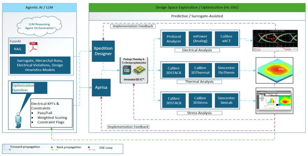
In Figure 1, the agentic AI can sit “above” the implementation and multi-physics engines to make DSE practical at the 3D-IC scale. The AI layer structures the optimization question into explicit electrical KPIs and constraints (pass/fail checks, weighted scoring, constraint flags), selects experiments, triggers tool runs, and uses surrogate/predictive models to reduce the number of expensive full-fidelity iterations. The same DSE loop can span three coupled workflows — electrical, thermal, and stress — so that improvements in one domain do not inadvertently create failures in another. The resulting insights and recommended design changes can be fed directly into the physical design flow, so tools, such as Xpedition™ and Aprisa™, can implement layout modifications that improve overall system performance, reliability, and manufacturability.
The agentic framework is enabled by a model context protocol (MCP) fabric, where specialized AI agents automate repetitive workflows, orchestrate tools and data, and allow engineers to focus on higher-value design and optimization activities. Figure 2 illustrates an MCP server–based “tool fabric” that sits between an agentic optimizer and the heterogeneous set of executables used in 3D-IC programs.
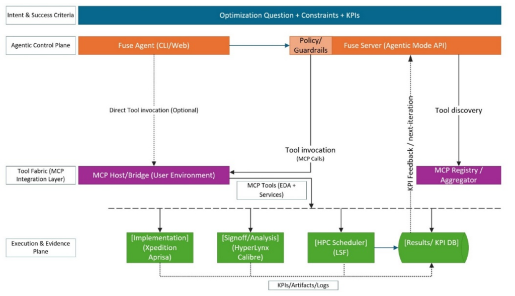
Instead of point-to-point integrations, each capability is exposed as an MCP server with well-defined inputs/outputs and registered for discovery. An MCP host/bridge mediates secure tool invocation, environment setup, data movement, and routing to local machines or HPC schedulers, while capturing logs, versions, parameters, and produced artifacts. This architecture enables scalable, multi-tool experimentation and closed-loop optimization by normalizing results into KPI/evidence stores and making every run traceable and repeatable across teams, sites, and tool chains.
Automated power and temperature-dependent scaling
In 3D ICs, power and temperature are tightly coupled, creating a non-linear feedback loop: temperature changes leakage and power, which in turn shifts temperature. To converge quickly and accurately, teams need a scalable way to generate temperature-dependent power inputs for thermal analysis without repeatedly re-running full characterization at every corner.
Temperature-dependent scaling flow shown in Figure 3 enables capturing baseline power at a single corner, building temperature-scaled libraries, mapping leakage vs. temperature at cell level, normalizing and generating multi-temperature power inputs, and closing the loop with 3D thermal analysis.
By eliminating the need for full re-characterization at every temperature point, the methodology significantly reduces runtime while maintaining high accuracy. This enables faster design space exploration, early hotspot detection, more effective thermal mitigation strategies, and improved optimization of power, performance, area, and reliability tradeoffs in complex 3D-IC designs.
AI-ready chip design data
The efficacy of AI models hinges on the quality and accessibility of their training data. 3D-IC design generates petabytes of heterogeneous data (layout, electrical, thermal, mechanical, manufacturing, design exploration results, simulation outputs, characterization data, PDK information) often residing in disparate, siloed systems with inconsistent formats or noise.
Making this massive, multi-domain data ready for AI requires deliberate investment in design data and IP management. Curating, labeling, and ensuring the quality and accessibility of data across the full design lifecycle is crucial. Scalable storage and compute platforms are also necessary as high-fidelity simulation outputs demand robust infrastructure.
Without these foundations, AI models risk learning spurious correlations, amplifying bias, or producing untrustworthy results. This highlights the importance of a holistic approach to data management within the EDA ecosystem.
Conclusion
As 3D IC systems grow increasingly complex and heterogeneous to meet the demands of the AI era, the synergistic combination of human expertise and AI-augmented design methodologies will be indispensable. Legacy chip designs are no longer sufficient to manage the massive parallelism and high-speed data movement required by modern AI workloads within strict power and thermal limits.
Siemens Innovator3D™ IC solutions use industrial-grade AI to help design teams handle these challenges. This AI approach supports human expertise, reduces manual workflow burden, and improves engineering throughput. It helps multiphysics validation keep pace with tighter PPA requirements and time-to-market pressure.
Advanced semiconductor design for AI increasingly depends on how well AI gets applied within the EDA ecosystem itself. By combining intelligent DSE, automated power and thermal co-analysis, and solid data management, Siemens 3D IC solutions help teams close designs faster without cutting corners, explore more design options without added risk, and deliver better silicon for next-generation AI systems.
About the Authors
Todd Burkholder is a Senior Editor at Siemens DISW. For over 25 years, he has worked as editor, author, and ghost writer with internal and external customers to create print and digital content across a broad range of EDA technologies. Todd began his career in marketing for high-technology and other industries in 1992 after earning a Bachelor of Science degree at Portland State University and a Master of Science degree from the University of Arizona.

Sudarshan Deo is a Software R&D Manager for 3D IC at Siemens Digital Industries Software. Sudarshan has expertise in implementing and integrating complex 3D IC workflows, including physical design, DFT, multi-physics, thermal, stress, SI, PI, DC IR-drop analysis, and advanced AI frameworks, and he serves as a technical point of contact for divisions across Siemens Digital Industries Software. Sudarshan holds an M.S. in Computer Science from California State University, Sacramento.

Dr. Muhammad Hassan is a Product Manager and Architect at Siemens EDA, where he spearheads cross-functional initiatives for 3DIC electrical analysis. His work centers on optimizing workflows and customer experience across the semiconductor ecosystem, from chiplet-level design to hyperscale data centers. A prolific innovator, Dr. Hassan holds over 40 U.S. patents and has authored more than 20 technical articles. He earned his Ph.D. in Electronic Circuits and Systems from the University of California, San Diego.