
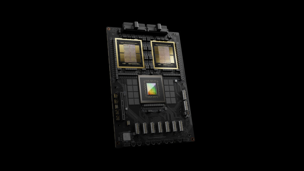
A kilowatt-class artificial intelligence (AI) accelerator can draw more than 1,000 A from a core rail below 1 V. Figure 1 shows NVIDIA’s GB200 Grace Blackwell Superchip, an example of the AI hardware that requires this high-current, low-voltage power delivery.
In a transient evaluation, a 16-phase regulator sees a load increase from 40 A to 360 A at 800 A/µs, a 0.4-µs rise. Controller delay and limited inductor current slew prevent the regulator from immediately matching that increase, with output capacitors supplying the current deficit as the regulator responds. If the core voltage falls below the processor’s operating limit during the transient, computation errors or a system crash may follow.
This article explains how multiphase voltage-regulator modules (VRMs) operate and improve transient response. It also discusses why load release can impose a tighter design constraint than load application.
How phases share the load
A VRM converts an input supply into the regulated voltage a processor requires. A multiphase design uses N synchronous buck stages connected in parallel to a shared output rail.
The controller maintains balanced current sharing, with each phase supplying approximately 1/N of the average load current during steady-state operation. It spaces switching events by 360°/N, allowing the inductor-current ripples to partially cancel at the output.
Balanced, evenly spaced phases produce combined ripple at N times each phase’s switching frequency. The amount of cancellation varies with duty cycle and differences between phases. VRM designers must check output ripple across the operating voltage range to ensure that ripple peaks remain within the processor’s voltage limits.
Increasing inductance reduces a phase’s ripple current and slows its response to load changes. Interleaving cancels part of the output ripple; designers can then lower per-phase inductance. Lower inductance allows current to rise or fall faster for a given applied voltage, reducing the current mismatch that causes voltage droop or overshoot.
What responds first
During a load increase, output capacitors supply the current deficit until the phase currents reach the new load demand. Their equivalent series resistance (ESR), which represents internal resistive losses, produces a voltage drop proportional to capacitor current. Equivalent series inductance (ESL), the parasitic inductance of the capacitor’s internal structure and terminals, adds a voltage drop proportional to how quickly that current changes.
As the capacitors discharge, their voltage also falls according to the equation ΔV = (1/C) ∫ (Iload − IVRM) dt. These effects overlap, although parasitic resistance and inductance often dominate the first voltage dip. A large capacitance value alone does not guarantee that the rail stays within the processor’s voltage limits during a fast load step.
The connection between the capacitor bank and processor adds inductance that further limits transient performance. If current through a 100-pH shared path rises at 800 A/µs, the inductive drop reaches 80 mV, or 10% of a 0.8-V rail. Notably, adding capacitors behind the same path does not remove its inductance. Instead, local decoupling and shorter current paths limit the resulting voltage drop.
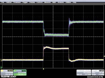
While the capacitors supply the current deficit, the controller responds to the voltage drop by increasing high-side conduction time. For N identical, uncoupled phases with all high-side switches on, the ideal total current slope is N(Vin − Vout)/L, where L is each phase’s inductance. Actual response also depends on switching restrictions and current limits. Figure 2 shows the output-voltage response during load application and release.
Table 1 summarizes the different constraints and design responses.
| Stage | Limiting factor | Design response |
| Initial capacitor response | Capacitance, ESR, ESL and path inductance | Local low-ESR, low-ESL decoupling and short current paths |
| Current ramp-up | (Vin − Vout)/L per phase | Lower inductance and added phases |
| Current ramp-down | Vout/L per phase | Lower inductance or TLVR; voltage positioning for overshoot margin |
| Phase re-addition | Detection delay and current sharing | Fast phase addition; test from minimum phase count |
Table 1. Transient stages, limiting factors and design responses in a multiphase VRM. Slope expressions assume identical, uncoupled buck phases and ideal switch states. L is the inductance of each phase.
Why load release sets the limit
A conventional buck regulator reduces current more slowly than it increases it when the output voltage is far below the input. With all low-side switches on, total current falls at N·Vout/L because each inductor sees only the output voltage. At 12 V in and 0.8 V out, the ideal ramp-up slope is 14 times the ramp-down slope.
For an illustrative design with 16 uncoupled phases at 150 nH each, a 320-A current change takes approximately 0.27 µs upward or 3.8 µs downward under ideal switching conditions (excluding controller delay). During load release, excess inductor current charges the output capacitors, producing voltage overshoot.
Adaptive voltage positioning (AVP) provides margin for these excursions by setting the output higher at light load and lower at heavy load. The rail starts nearer the upper voltage limit before a load increase and nearer the lower limit before a load release. In AI accelerator core supplies, AVP can reduce the required bulk capacitance, provided the programmed voltage variation stays within the processor’s load-line specification.
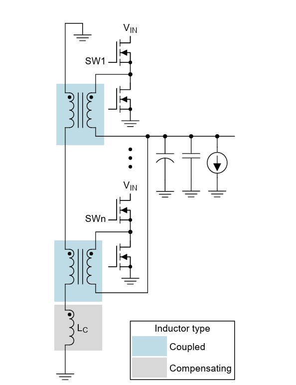
Trans-inductor voltage regulators (TLVRs) accelerate the current response through a shared loop connecting secondary windings on the phase inductors, as shown in Figure 3. This coupling produces lower effective inductance during transients than during steady-state operation. Reducing the loop’s compensating inductance further accelerates the response but increases ripple.
The added ripple raises root-mean-square (RMS) current in the power stages, increasing conduction losses. To meet transient voltage limits within the board’s thermal budget, VRM designers weigh the reduction in output capacitance against the additional power-stage losses and cooling requirements.
What phase shedding changes
At light load, switching and gate-drive losses account for a larger share of total converter losses. Phase shedding reduces these losses by disabling unnecessary phases. The remaining phases supply the load current while maintaining voltage regulation.
Fewer active phases initially limit the regulator’s current-slew capability during an abrupt load increase. The controller reactivates additional stages, though uneven current sharing during this transition risks driving an individual inductor into saturation.
An all-phase peak-current rating does not establish this transient performance. Designers verify the response with load-step tests starting from the minimum permitted active phase count, measuring voltage undershoot and individual phase currents.
For TLVRs, disabling a phase stops its switching but does not disconnect it from the coupled magnetic network. Secondary-loop current can still induce current through that phase’s MOSFET body diodes when both switches are off. Phase shedding saves power only if the avoided switching losses exceed the added conduction losses.
Summary
Multiphase VRMs on AI accelerator boards increase current capacity and support faster current response. Capacitor characteristics and path inductance determine the initial voltage excursion. In conventional buck stages, the low output voltage limits current ramp-down, often imposing tighter demands on load-release performance.
Interpreting measured undershoot and overshoot requires defined load-step conditions and the initial active phase count. A peak-current rating or load-increase test is insufficient to establish whether the rail stays within the processor’s voltage limits. VRM designers must use these measurements to verify rail compliance, while AI data center operators require system-level validation that accelerators remain stable through workload transitions.
References
Optimal Design for an Interleaved Synchronous Buck Converter Under High-Slew-Rate, Load-Current Transient Conditions, Texas Instruments
Multiphase Buck Design From Start to Finish (Part 1), Texas Instruments
Introduction to the Trans-Inductor Voltage Regulator (TLVR), Texas Instruments
How to Balance Current Using Multiphase Converters, Texas Instruments
Impacts of Transients on AI Accelerator Card Power Delivery, Analog Devices
Considerations for the Output Current and Voltage Ripple in a Multiphase Buck with Coupled Inductors, Analog Devices
Improve Two-Phase Buck Converter Performance with a Coupled-Choke Topology, Analog.com
Load Transient Response Testing for Voltage Regulators, Analog.com
Improving Buck Regulator Transient Response with TLVR, Flex
AI Load Dynamics–A Power Electronics Perspective, arXiv
Related EEWorld Online content
How TLVRs Support Extreme Power Demands in AI Datacenters
What are the Different Types of AI Accelerators?
What are the Hardware Strategies for Building Energy-Efficient AI Accelerators?
How to Minimize Design Cycles for AI Accelerators with Advanced DFT and Silicon Bring-Up
What are the Different AI MLPerf Benchmarks from MLCommons?