
Nick Perosino, New Product Development Manager at Central Semiconductor (an AEM Company), recently presented a webinar on using bare die to solve space, electrical, and thermal constraints in discrete power designs. In Part 1 of this two-part Q&A, he makes the case for why design engineers should be paying closer attention to bare die and what they stand to gain mechanically and electrically.
Q: What exactly do you mean by “bare die,” and what forms does it come in?
A: Bare die is basically a blanket term for anything referring to the chip or die inside a semiconductor component. You’re actually talking about the silicon component, or in the case of wide bandgap semiconductors, the gallium nitride on a silicon chip, or the silicon carbide chip. When I say bare die, that’s all I mean. It’s just an industry term for the chips or die inside the components.
The key with bare die is that they’re extremely flexible. It can start with unsawn wafers, sawn die on tape, sawn die in a gel pack, sawn die on UV release tape, or sawn die in a tray. All of those constitute bare die. That also plays into the manufacturability side of things, because depending on whether you’re running a manual, semi-manual, or automatic assembly process, that’s your first consideration for how these chips are being handled and placed.
Q: What are the three core problems that bare die can solve?
A: Bare die can really solve three key problems relating to mechanical, electrical, or thermal issues. Mechanical is pretty black and white; it’s really based on space savings. Electrical and thermal are a little less black and white, and a little more about how you use them. The idea is that, instead of buying one-size-fits-all components off the shelf that are already assembled a specific way, using bare die gives you the power to change how you want to assemble it and lets you optimize your assembly to get the best output possible for your application. That’s not something manufacturers always consider when they’re putting out product lines, because they’re selling into a bunch of different applications to a bunch of different customers. At the end of the day, purchasing a bare die gives you the most control over your application and your product.
Q: How significant are the footprint savings in a real design?
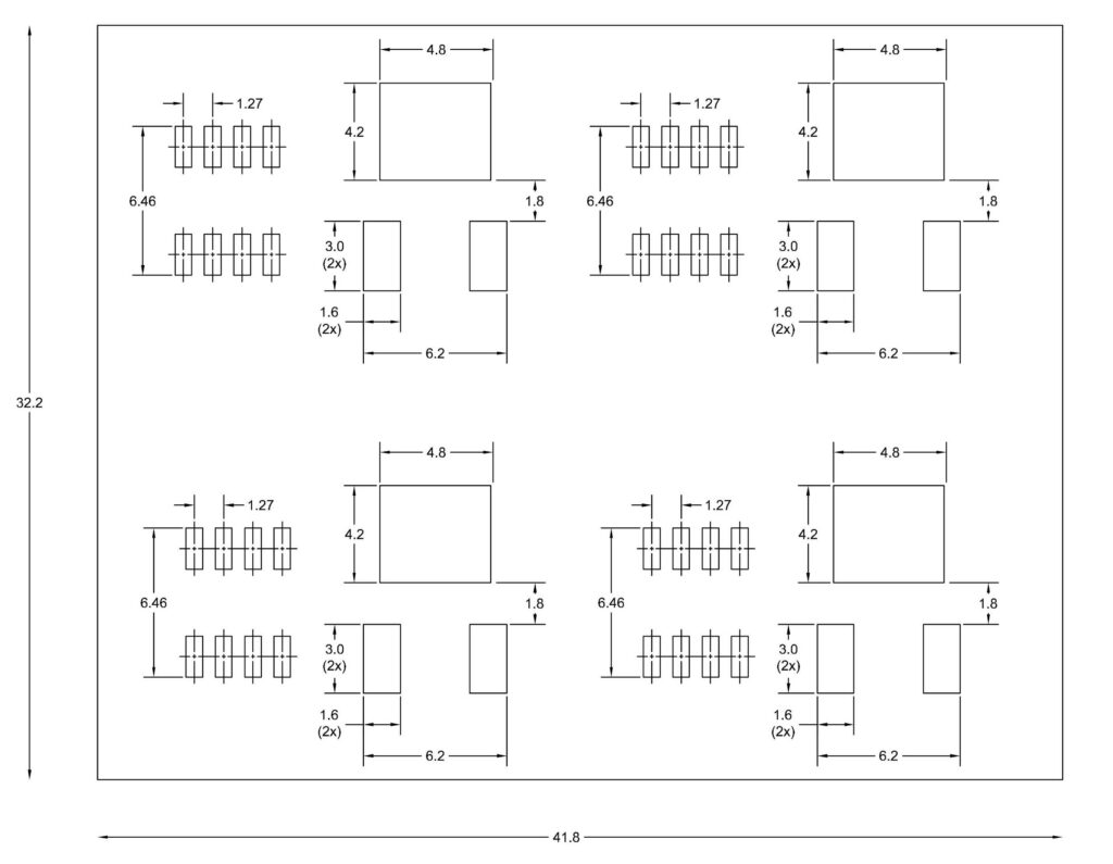
A: I took a pretty foundational design: the bidirectional boost-buck converter. We’ll take one single-channel gate driver per FET and four MOSFETs, assuming a TO-252 for the MOSFETs and an SOIC-8 for the gate driver. This isn’t including any passives: no gate resistor, no bootstrap cap, no filter caps, no inductor. Just the active semiconductor components. Based on proper spacing and recommended mounting pads, you’re looking at about 42 by 32 millimeters minimum.
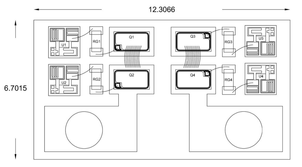
Now, what if you switch to a bare die? The same configuration, four MOSFETs at 40 volts, 105 amps, 1.75 by 1 millimeters, and gate drivers at 1.5 millimeters square, placed in a hybrid cavity, and this time we also include the gate resistors and the inductor. You end up with only a 6.7 by 12.3 millimeter footprint. You’re talking about roughly a third in the x-direction and about a fifth in the y-direction of what you were looking at before. That’s a real-life example I’ve seen in my career, where someone was building something just like this, and the suggestion was made to move to a hybrid bare die design, and it ended up saving them a lot of space.
Q: Why do packaged components introduce parasitic resistance, and how much does it actually matter?
A: The first and most important thing in package parasitics is the bond wire configuration. Bond wires can be a huge pain; they add resistance, and they’re going to add stray inductance, which is really brutal for switching-based designs because you get all sorts of transients and spiking.
Take an SOT-23 using two 1-mil copper wire bonds and a copper lead frame, very boilerplate, standard assumptions for what you’d see every day. For a 1A diode, the addition from parasitics comes out to about 10 millivolts. That could be a deal-breaker in some cases, like if you’re trying to match parasitics in a parallel configuration. Take a MOSFET assembled the same way, and you’re going to add 10 milliohms. That’s a lot of extra impedance. 10 milliohms can translate to nearly 10-plus lost amperes in maximum current.
Q: Can you meaningfully reduce those parasitics without changing the package footprint?
A: If you buy it as bare die and implement it in a hybrid, you can stick with the same lead frame paddle, so you’re not increasing footprint size, and you’re still going to use wire bonds. But what happens if you upgrade to 2-mil copper instead of 1-mil, and upgrade your wire count to four? You’ve just provided more parallel resistance paths to reduce the total impedance of the system.
Why wouldn’t the manufacturer do this? If they have ten different applications they sell into and a hundred customers within those applications, and their main off-the-shelf construction works for 75% of them and is optimized from a pricing and logistics standpoint, there’s no real need to change it. But you might fall into that 25% it’s not optimized for. If you make that change using a bare die, your new parasitics are one-fifth of the old: 2 milliohms added resistance for a MOSFET, and 2 millivolts added forward voltage for a diode. Two millivolts is essentially negligible, and two milliohms means you’re maybe only going to lose an amp or an amp and a half off the total max current you can achieve with the MOSFET.
Q: Can assembly design also affect switching transients?
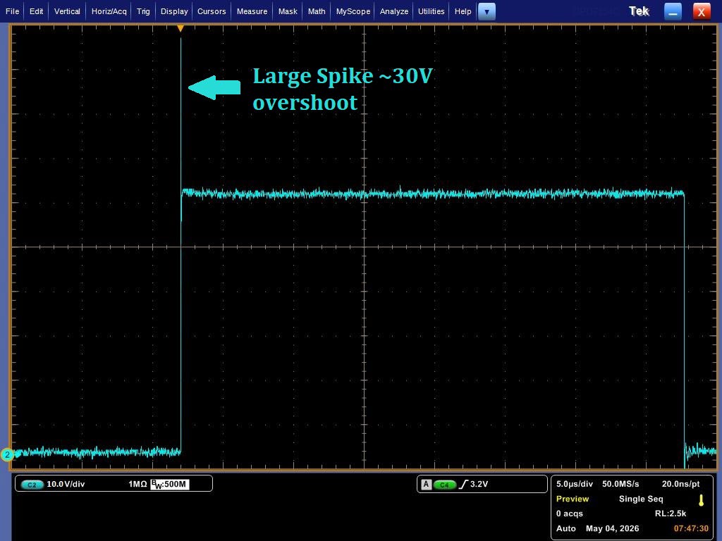
A: Parasitic inductance is one of the most common issues I see causing faults in switching-based systems. With a standard packaged component, 95% of the time, it’s going to be cylindrical wire bonds with significant loop height and wire length. We tested a 100V power MOSFET off the shelf, not optimized for switching, and saw a 30-volt overshoot from the intended value. That could damage other components in the circuit, or even the FET itself.
Take the same FET and implement it in a hybrid with a ribbon bond, still not optimized in any extreme way, just a small change. All we’ve done is replace the wire bonds with a flat ribbon bond that’s not going to have as high a loop height, and because it’s flat, there’s more surface area making contact with the topside of the die. We see a 20-volt reduction in overshoot from that one modification. Hybrid designs also make it very easy to integrate RC snubbers within the same package cavity as the FET die, which gives additional protection against transients.
In Part 2, Perosino walks through how bare die assembly decisions directly impact thermal resistance and current capability, when it makes sense to request a custom die layout, reliability qualification under MIL-PRF-38534, and what’s really holding engineers back from making the switch.