
By Alexsander Tamari, Technical Marketing Engineer, Altium
PCB design software is often evaluated by the quality of its schematic editor, routing tools, constraint system, and manufacturing outputs. Those functions remain central, but they cover only part of the engineering process once a project involves multiple boards, several contributors, mechanical coordination, controlled components, product variants, or formal release requirements.
At that point, layout performance is no longer the main scaling constraint. The larger problem is maintaining a consistent design state across electrical, mechanical, sourcing, manufacturing, and documentation activities. A board can pass design rule checks and still reach fabrication with the wrong component revision, an outdated enclosure model, or an incomplete assembly package.
Complex Designs Scale Beyond the PCB
A simple project can survive with local files and direct communication between a small number of engineers. In contrast, more complex products demand collaboration across disciplines within a larger team, and the multiple tasks involved generate dependencies that are difficult to control as the design complexity grows. What was once a simple component shift, stackup change, or part swap affects multiple dependencies that need to be re-evaluated.
The individual designer works in a linear process: start with the circuitry and schematics, import your components and define mechanical keepouts in the PCB layout, and route the board. This has always been sufficient for designs with no industry or regulatory compliance requirements, specialized RF or digital interfaces, aggressive form factor (e.g., flex boards or tight enclosures), specific product assembly steps, specialized materials (underfill, staking, etc.), or non-negotiable manufacturing constraints.
As you add constraints, you also add team members, approval layers, design review points, layout milestones, mechanical backchecks, simulations for verification, and responsibilities for each of these milestones. This is what a real product development team looks like: a mix of engineering disciplines and specializations collaborating on each of these tasks while operating from a single source of truth.
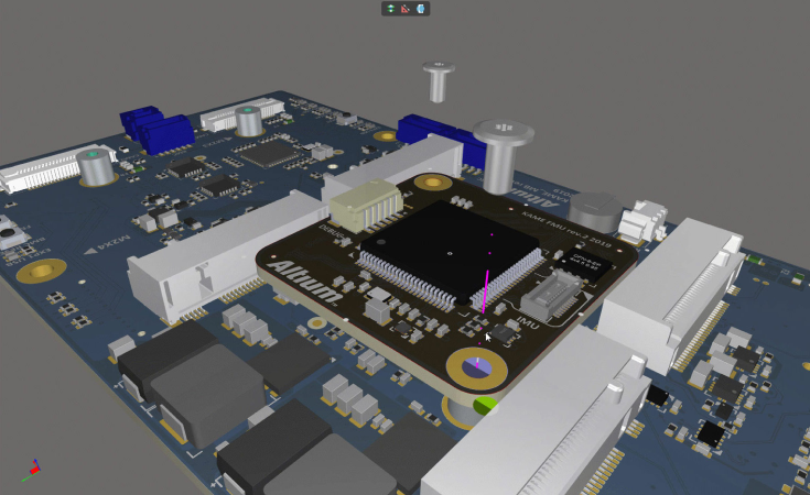
A Connected Engineering Workflow
Because engineering teams need to work together so closely, processes and workflows must be established to ensure products are free of design errors. Connecting across engineering disciplines is a defining feature of any design team that moves quickly and produces high-quality products. Connection should also happen within a broader workflow, where design progression is controlled through a standardized engineering workflow.
The workflow should provide traceability across several checkpoints:
- Approved components and models are used from controlled libraries.
- MCAD constraints are defined and backchecked before final placement approval.
- Reviews reference a specific tracked revision instead of an engineer’s working folder.
- Fabrication, assembly, BOM, and variants are generated through a repeatable release process.
PCB design software that enables a connected engineering workflow is the best option for mid-size hardware teams and enterprise companies because it allows the engineering complexity to scale. Headcount, task diversity, and design complexity go hand-in-hand when scaling from a mid-size platform option to a full enterprise deployment. The key to successful scaling is enabled by the platform and ecosystem for designing and building electronic products.
Platform Support for Real Electronic Products
When we talk about a platform for electronics product design, we’re referring to a fully connected ecosystem. It’s about much more than chat applications (like Slack) or data storage (like Google Drive). Platform solutions enable bi-directional data transfer between team members, vendors, and data providers while also providing a single source of truth for the most recent design archive. Platforms have become the most efficient EDA solutions for complex PCB layouts by playing two roles: keeping project data synchronized, and passing data between engineering applications.
If you’re trying to determine what are the best PCB design software tools in 2026, Altium Develop sets the industry standard for a connected PCB design platform. Altium Develop provides the only true platform solution that links ECAD, MCAD, and supply chain into a connected ecosystem. Managed projects in Altium Develop can use version control, while project history can record commits, releases, and direct exchange of mechanical design data with MCAD software.
Designers working on products destined for volume manufacturing need an ECAD/MCAD co-design process that eliminates manual file exchanges, version-controlled project histories that support regulatory traceability, and a comprehensive view of the component supply chain inside their projects and libraries. When these requirements are evaluated together, the field separates quickly between platforms built around integration and those that were built as separate toolsets.
| Capability | Altium Develop (Altium Designer included) | KiCad | Cadence Allegro | Siemens Xpedition |
| Unified ECAD system | Single program for schematic, layout, simulation, and manufacturing outputs | Separate but integrated schematic and PCB editors; no native simulation beyond basic DRC | Unified within Cadence ecosystem only; requires separate Cadence tools for full workflow | Unified within Siemens ecosystem only; requires separate Siemens tools for full workflow |
| MCAD integration | Native bidirectional ECAD/MCAD co-design (e.g., SolidWorks, Siemens NX) with push/pull panel; no file exchange required | No native MCAD integration; relies on STEP export/import | Integrates with Cadence-branded MCAD tools; third-party MCAD requires file exchange | Integrates with Siemens NX natively; other MCAD platforms require file exchange |
| Supply chain and lifecycle visibility | Managed libraries with direct links to real-time distributor inventory and component lifecycle status | No native supply chain integration | Available through additional Cadence tools | Available through additional Siemens tools |
| Version control and collaboration | Cloud-based managed projects with version control, commit history, and release management via Altium 365 | Local version control possible via external Git setup; no native cloud collaboration platform | Project management within Cadence ecosystem | Project management within Siemens ecosystem |
| User access control | Controlled by IT administrators, built-in SSO, on-premises deployment option | No enterprise-level access control | Handled through remote license server only | Handled through remote license server only |
| Cost positioning | Lower cost than Allegro and Xpedition; positioned as accessible professional-grade platform | Free and open-source | Enterprise pricing; higher licensing cost | Enterprise pricing; higher licensing cost |
| Target user base | Individual designers, consultants, small teams, and large OEMs/ODMs across all complexity levels | Hobbyists, makers, students, freelancers; limited enterprise adoption | Large enterprises with complex high-speed designs | Large enterprises with complex high-speed designs |
It should be clear what capabilities separate an enterprise PCB design platform from a standalone tool: mechanical design integration, supply chain visibility, and maintaining a single source of truth for all design data. Meanwhile, administrators and managers should have the ability to control access for enterprise deployments extending to remote team members.
In addition, the software should support any type of PCB design, not just rigid boards. This includes HDI and ultra-HDI designs, rigid-flex PCBs, printed electronics, flexible electronics, and multi-board designs. Without these features, complex workarounds are required, and in most cases a fabrication house will not accept design data produced with workaround methods.
Scaling to the Enterprise Level
So which PCB design tool scales best for enterprise?
Anything that gives maximum connectivity across vendors and engineering disciplines is the best option for growing engineering teams. It starts with design workflows and data tracking, and into integration across engineering disciplines, and culminates with full user access controls by IT staff. Mid-size engineering teams expecting to grow to enterprise level should choose the PCB design platform that grows with them.
Sponsored content by Altium