
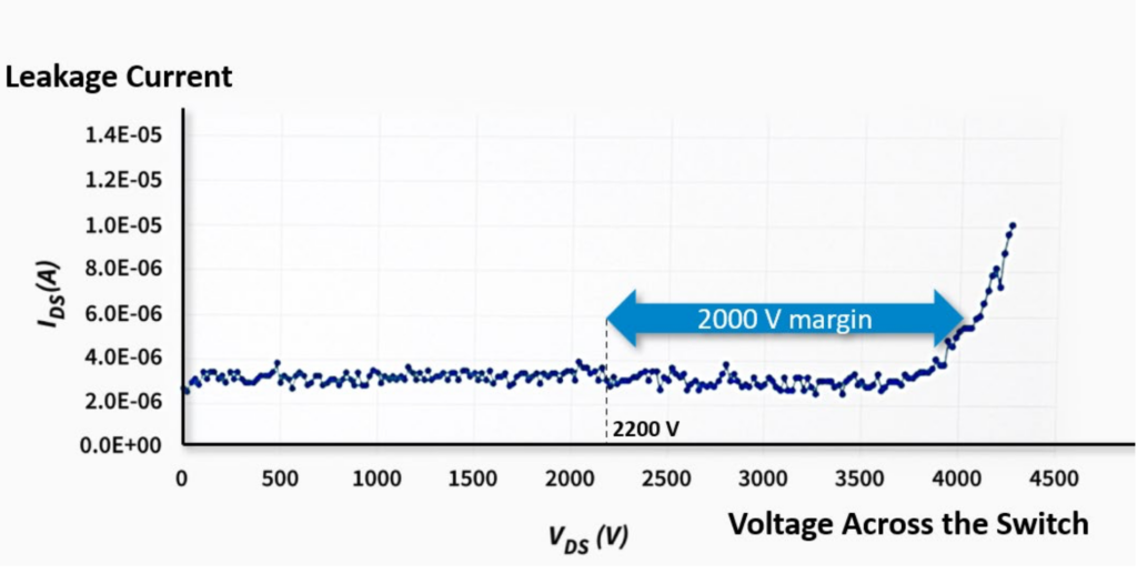
Power Integrations has announced a 2200 V GaN switch technology, extending PowiGaN gallium-nitride beyond the voltage ceiling of commercially available GaN today. The company is positioning it for AI data centers, EVs, photovoltaics and HVDC infrastructure as those markets push toward higher-voltage bus architectures for greater power density.
PowiGaN at 1700 V is already designed into single-stage data center auxiliary power, and 1250 V PowiGaN offers what the company maintains is a simpler alternative to stacked GaN in the main 800 VDC power path. EEWorld Online talked through the engineering behind the 2200 V step with Roland Saint-Pierre, VP of product development, covering the sapphire substrate tradeoffs, the cascode architecture, and how it stacks up against SiC on switching frequency and cost.
You use a sapphire substrate for PowiGaN, which isn’t standard for high-voltage GaN. What tradeoffs come with sapphire versus GaN-on-silicon at this voltage class? Thermal performance, cost, yield?
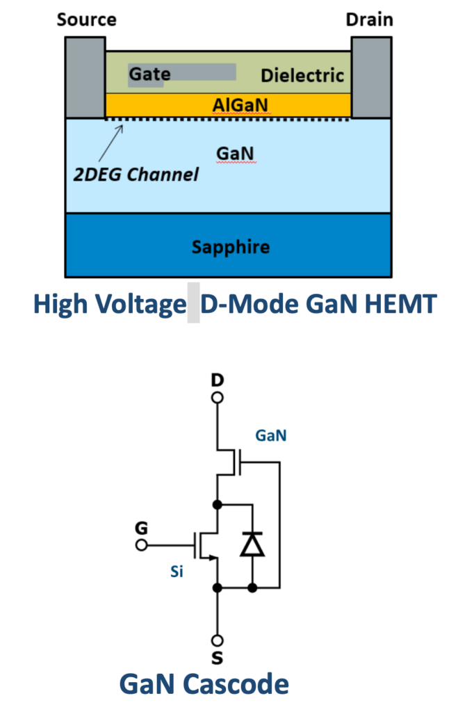
The big advantage is our ability to scale voltage. We started on sapphire at 750 V, and with that substrate, plus epitaxial engineering, we’ve kept scaling: 750, 900, now 2200 V. The tradeoff is thermal, sapphire isn’t the best conductor. But it’s also insulating, which lets us fully isolate the device. The heat sink sits at source potential instead of switching at high voltage, so we get less EMI and a simpler design.
PowiGaN uses a cascode arrangement instead of E-mode GaN. What’s the practical design advantage?
Our GaN HEMT is D-mode, normally on, so it’s paired with a low-voltage silicon MOSFET, you drive the MOSFET’s gate for on-off behavior. E-mode GaNs are finicky about gate voltage and often need a negative drive in a half-bridge because of low threshold voltages. PowiGaN doesn’t have that problem, much wider gate-drive compliance, no negative drive needed, fast to adopt with low design complexity.
How much of a switching-frequency advantage does GaN have over SiC, and what does that buy designers?
GaN can operate above 1 MHz; the max I’ve found for SiC is around 250 to 300 kHz. Higher frequency lets you shrink the magnetics for much higher power density, especially in zero-voltage-switching LLC designs where there’s only conduction loss and magnetics size dictates density.
You just released this. Do you have fit-rate data for the 2200 V device itself?
Good point. This is a technology announcement, not a product announcement. We’re working on that data now, but we’ve cleared enough internal milestones to be confident deploying it into product development.
If a company’s committed to SiC for 800 V designs, will a comparable 2200 V GaN device cost more?
Vertical GaN should eventually displace SiC at all voltage and power levels, though that’s not what we’re addressing today. SiC fabrication is intensive, so vertical GaN should be cheaper long term. What we’re disclosing now is 1250 V, 1700 V and 2200 V PowiGaN, which displaces SiC at lower power levels, more cost-effectively.