
By Joshua Rubin, Advanced Packaging Technologist
Q: Are chiplets simply an evolution of multi-chip modules (MCMs) from the 1990’s?
A: In many ways, yes. Early multi-chip modules, such as IBM’s 9121 from 1991 and even earlier thermal conduction modules (TCMs) from the 1980s, already demonstrated heterogeneous integration, disaggregated architectures, and system-in-package (SiP) concepts. These designs combined CMOS static RAM (SRAM) cache chips and bipolar logic chips on complex ceramic substrates. Through the 2000s, heterogeneous integration expanded further as separately manufactured components such as processors, memory, sensors, and other diverse components were assembled within a single package. By the 2010s, the industry began to consolidate around what is now explicitly defined as chiplet-based design. Putting aside the nuances of the nomenclature, it is important to recognize that the industry has dramatically accelerated the enablement, standardization, and productization of chiplet-based hardware.
Q: Is there any practical difference between designs based on MCMs vs those based on chiplets?
A: The practical distinction between traditional MCMs and modern chiplets lies not in modularity alone, but in scale, interface, and ecosystem maturity. Chiplets today span an enormous range in size and function, from small, specialized dies (10’s of mm2) to full reticle-scale compute tiles (~858 mm2), and support CPUs, GPUs, AI accelerators, memory, IO, photonics, sensors, and more. They are deployed across both standard and advanced packaging platforms, including interposers, bridges, fanout, and 3D integration. Critically, advanced packaging has enabled chiplets to be placed within tens of micrometers of one another, supporting aggressively scaled interconnects and new classes of low-power, high-bandwidth, low-latency die-to-die interfaces such as Universal Chiplet Interconnect Express (UCIe) and bunch-of-wires (BoW). These interfaces, whether custom or industry-standard, are increasingly central to chiplet architectures, enabling communication characteristics that approach on-die interconnects, especially in 3D designs with hybrid bonding (10 micron interconnect pitch or less). In short, while chiplets are rooted in MCM and heterogeneous integration concepts, they represent a step-change in architectural capability driven by advanced packaging, standardized die-to-die interfaces, and a rapidly maturing industry ecosystem.
Q: What are the main drivers for chiplets?
A:
- Cost and yield at advanced nodes: Monolithic dies at leading-edge nodes are prohibitively expensive and yield-limited, especially for large dies like those used by hyperscalers and Nvidia. Chiplets reduce the die size, improve yield, and allow selective use of advanced nodes only where they deliver value.
- System-level scaling beyond Moore’s Law: While traditional transistor scaling in advanced nodes no longer provides sufficient PPA (power, performance, area) scaling alone, chiplets enable “more-than-Moore” scaling through architectural composition, high bandwidth die-to-die interconnects, and advanced packaging.
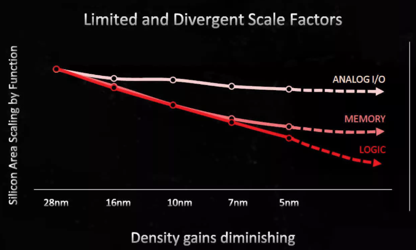
- Heterogenous integration and node optimization: Different functions (logic, memory, analog, I/O, RF) scale differently and benefit from different process technologies (see Figure 2). Chiplets allow best-fit process selection per function, thereby improving PPA.
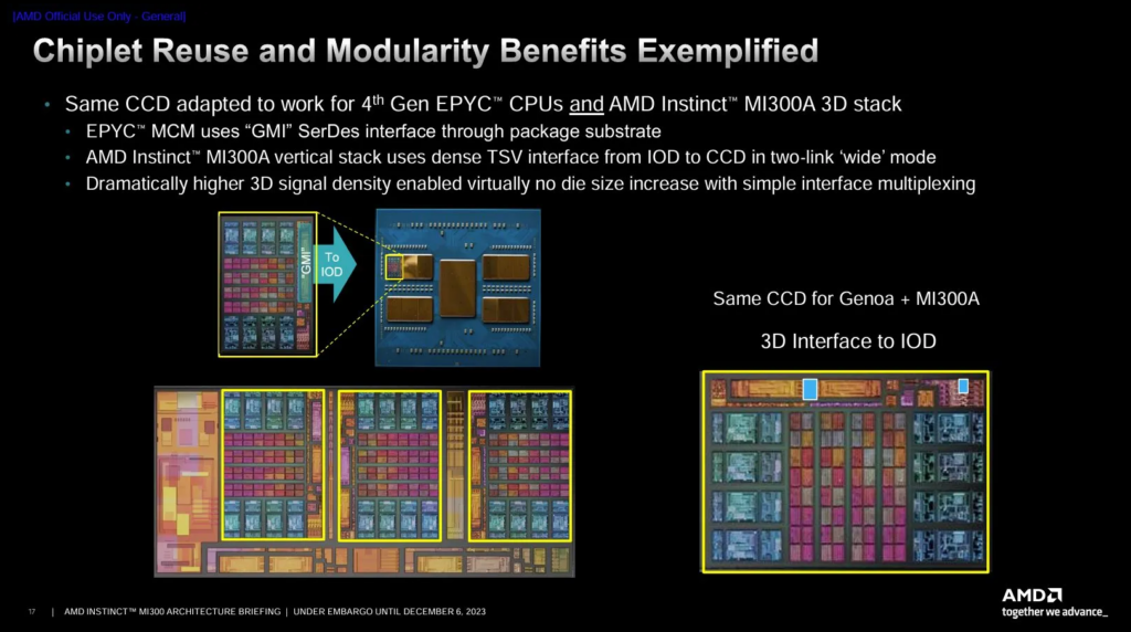
- Design reuse, time-to-market, and risk reduction: Reusable chiplets shorten development cycles and reduce risk. Parallel development enables faster product ramps and easier SKU differentiation for products. A particularly compelling example of this approach can be seen with the use of nearly identical CCDs (Core Compute Die) in a 3D configuration in MI300A and a 2D configuration in the 4th-Gen EPYC Genoa processors. CCDs contain different IOs for both 3D and 2D communication, which is enabled by different Far-back-end-of-line metal termination (hybrid bond vs bump) and interface multiplexing (see Figure 3).
Overall, chiplets are driven by economics at advanced nodes, the need for system-level scaling, heterogenous integration, and faster, lower-risk product development.
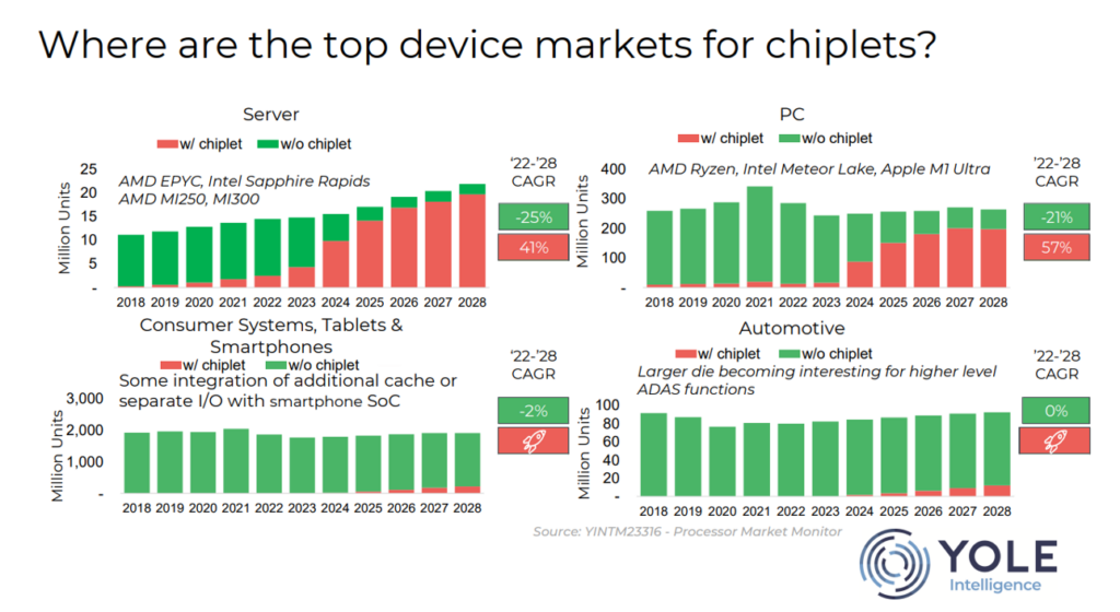
Q: What are some of the really big application drivers for chiplets?
A:
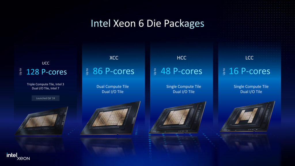
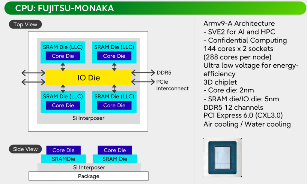
Data center & high-performance CPUs: CPUs are employing chiplets in different architectures. For instance, Intel Xeon 6 uses a disaggregated tile architecture with separate compute and I/O tiles to enable better scalability and yield. Compute tiles are fabricated on a more advanced node, while I/O tiles are on a more mature, cost-effective node. I/O tiles are reused with varying numbers of compute tiles (see Figure 4) to generate different SKUs, thereby enabling faster derivatives and products that can exceed the scale and performance of monolithic designs. Fujitsu’s upcoming Monaka processor will use a 3.5D architecture with a 3D many-core architecture, whereby 2nm cores are stacked above 5nm last level cache SRAM dies, and multiple 3D tiles are coupled to an adjacent I/O tile. Xeon 6 and Fujitsu Monaka follow two different chiplet architectures, distributed I/O (at edge of chiplet array) vs central I/O (hub chiplet). AMD Ryzen and Epyc follow similar chiplet trends.
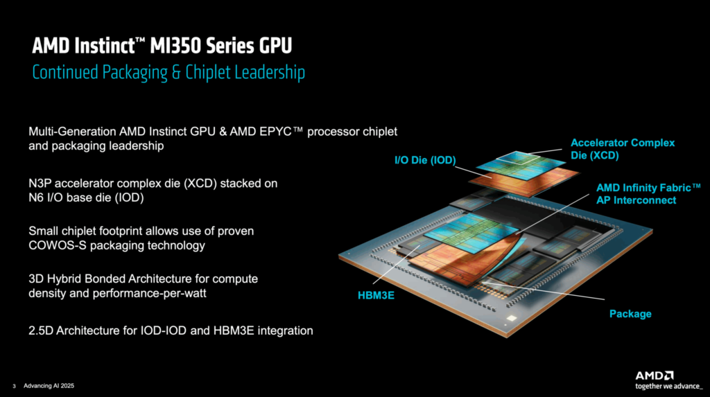
AI accelerators and GPUs: With HBM being pervasively used for training hardware, most of the latest AI hardware is chiplet-based, including Nvidia’s upcoming Rubin GPU. AI hardware requires aggressive scale-up. Placing more compute and memory on a given package helps achieve this goal. Chiplet-based AI hardware use 2.xD, 3D, and 3.5D packaging in a similar fashion to the CPU cases. Nvidia Rubin uses two reticle-sized compute chiplets (3nm) flanked by two dedicated I/O tiles (5nm) in a disaggregated I/O architecture. Whereas AMD’s MI355X follows a hub-like chiplet approach in 3D. Four XCD (3nm compute dies) are stacked on a common I/O base die (6nm) that also contains AMD’s Infinity Cache (see Figure 5). Furthermore, a 3.5D architecture is utilized, whereby two base dies are connected with proprietary Infinity Fabric die-to-die links having 5.5TB/s bisectional bandwidth and multiple HBM3e stacks flank the I/O base dies. These examples of Nvidia and AMD hardware harness TSMC’s most aggressively scaled 3D SoIC, CoWoS-S, and CoWoS-L technologies.
Co-Packaged Optics (CPO): As the industry shifts from traditional pluggable transceivers to co-packaged optics, new opportunities abound for chiplets. CPO brings the optical interface in close proximity to the edge of the ASIC, thereby enabling higher density on-package signal routing between the optical transceivers and the ASIC. By eliminating the high-speed electrical I/O bottleneck on the PCB, higher I/O bandwidth at lower power can be achieved. CPO is ripe for chiplets due to the need for heterogenous integration and the benefit of high-bandwidth die-to-die interconnectivity for this application. Early products integrate Photonic Integrated Circuits (PIC) on one die and Electronic Integrated Circuits (EIC) on another die. With Ayar Labs announcing the world’s first UCIe-enabled Optical Chiplet for AI scale-up in 2025, numerous key players such as Nvidia and Broadcom are also making product announcements with CPO. CPO clearly has big implications for PCB and system design. Drawers heavily utilizing CPO will have a reduction of long high-speed electrical traces and retimers on the PCB. On the other hand, fiber routing becomes a primary system design concern.
Advanced Driver Assistance Systems (ADAS) and automotive applications: Whether it is ADAS, infotainment systems, or EV control systems, numerous automotive applications can potentially benefit from chiplets. ADAS is an application that greatly benefits from heterogeneous compute. Separate chiplets can potentially support distinct workloads – digital signal processing chiplets for sensor data (e.g., LiDAR), AI accelerator chiplets for vision/ML inference, and CPU chiplets for general processing. Multiple chiplet initiatives have been formed in the industry to address the automotive application space.
Q: What about High Bandwidth Memory (HBM)? Is that a chiplet?
A: The debate over whether HBM is a true chiplet or merely an advanced memory component represents a fundamental shift in how we define silicon architecture. On one hand, HBM is the “poster child” for the chiplet ecosystem, having successfully pioneered the standardization (through JEDEC) of interoperable sockets that allow different manufacturers’ memory stacks to be “plugged into” diverse processor packages. By vertically integrating multiple DRAM dies into a single 3D stack that sits on an interposer alongside compute cores, HBM functions as a modular building block that enables heterogeneous integration.
Critics argue that HBM lacks the full “design freedom” of general-purpose chiplets; it is a rigid, specialized subsystem where the logic layer serves only to orchestrate signals rather than perform independent compute. However, as the industry moves from 2025 to 2026, the rise of custom HBM solutions and standardized interconnects like UCIe is blurring this line further, potentially transforming HBM from a simple memory tile into a co-designed processing element. Ultimately, HBM’s status as a chiplet may be less about its internal architecture and more about its role as the industry’s first successful blueprint for a modular, standardized, heterogeneously integrated component. Other chiplet-based memory modules are destined to show up in the industry based on 3D-stacked SRAM, emerging memories (e.g. resistive RAM, magnetic RAM), or processing-in-memory (PIM).
Q: What technology is needed to enable chiplets?
A: In brief, since this has been covered extensively in literature, there are a few key enablers:
- Advanced packaging: There have been some chiplet designs based on standard packaging, but advanced packaging enables higher bandwidth, lower energy per bit, and shorter interconnect latency.
- High-bandwidth die-to-die interconnects and standardization: Although many of the early chiplet-based designs use proprietary die-to-die links, open standard interfaces like UCIe and BoW are quickly gaining traction. Ultimately, open standard interfaces are going to be essential for achieving an open chiplet marketplace. The industry is pursuing a long-term vision of a plug-and-play ecosystem at the silicon level, whereby designers would be able to seamlessly mix and match chiplets from different process nodes and suppliers.
- Known Good Die (KGD) and test infrastructure: Complex multi-die packages need new test infrastructure to guarantee that the added cost and complexity of advanced packaging don’t outweigh the yield benefit of chipletization.
- Electronic Design Automation (EDA): There are multiple new challenges that EDA vendors must address to enable a successful chiplet design. Aside from multi-die floor-planning, package-aware signal and power integrity, and cross-die timing and functional verification, there are other unique aspects that push complexity beyond traditional SoC flows. Additional challenges include mechanical and thermal analysis for new packaging form factors. Complex multi-chiplet architectures introduce new challenges in test strategy definition, test-point insertion, and design security, particularly in multi-vendor environments.
Q: How will future chiplet innovations impact package, board, and system design?
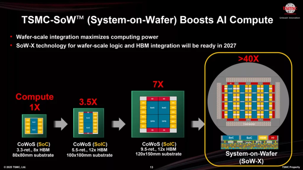
A: One only needs to look at TSMC’s packaging roadmap (see Figure 6) to begin to grasp the enormous impact that scaled chiplet architectures will have on package, board, and system design. Wafer-scale integration is poised to completely upset traditional board and system design. Whereas Nvidia’s Rubin GPU may have an interposer that is ~5x reticle (5 x 858 mm2), Rubin Ultra will most likely align with the next stop on the roadmap at ~9.5x reticle in size. When considering such a large interposer, the substrate (package) carrying the interposer can actually start to exceed the dimensions of PCIe card form factors and standardized mezzanine card dimensions, such as OAM (open accelerator module).
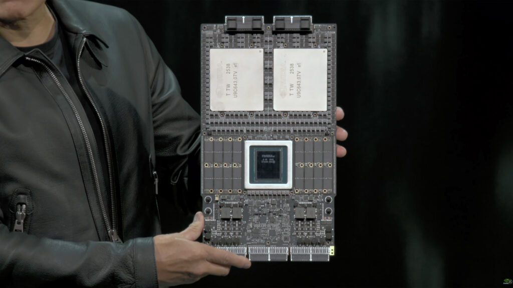
Looking back at Nvidia Blackwell and the recently announced Nvidia Vera Rubin platform, you can start to see the shift in package and card design practices – massive packages mounted directly on boards (see Figure 7) without intermediate mezzanine cards. This practice places new design constraints on fanout wiring on package and BGA pitch. Nvidia is leading the charge towards 1MW server racks. Ultimately, as we trend towards wafer-scale compute and then panel-scale compute, the chiplet array will approach board dimensions. Vertical power distribution clearly becomes necessary at such large scales, while I/O, cooling, and mechanical design will need to change dramatically to accommodate this massive shift in chiplet scaling. Meanwhile, hybrid bonding and 3D integration continue to further blur the line between chiplet and package design.
The future portends to be a very exciting time to be in chiplet, package, board, and system design.
About the Author

Joshua Rubin is an advanced packaging technologist and former Senior Engineer at IBM, where he served as technical lead on projects dealing with wafer-scale 3D integration, system performance analysis for novel technical elements, heterogeneous integration, and AI hardware design. As an IBM Master Inventor, he holds over 100 patents in transistor design and integration, power distribution, 3D integration, advanced packaging, and memory devices. He earned his PhD in electrical engineering at Cornell University and has published extensively, with presentations at leading conferences including the Electronic Components and Technology Conference (ECTC), IEEE Journal of Solid-State Circuits (ISSCC), IEEE Electron Device Letters (EDL), and IEEE International Conference on MEMS. Most recently he was a technical lead for the packaging and card design of IBM’s latest Artificial Intelligence Unit (AIU) product.
References
Chiplet Technology: Disrupting Chip Design and Fueling Growth | TechInsights
Co-Packaged Optics – Heterogeneous Integration of Chiplets (Switch, Photonic IC, and Electronic IC) | Published in Journal of Microelectronics and Electronic Packaging
Embedded – Chiplet Technology in Automotive Applications: A Cost-Effective Path to Advanced Electronics
How do you test chiplets?
Can chiplets save the semiconductor supply chain? – Electrical Engineering News and Products