
In part 1 of this series, we looked at the high-speed serial interfaces—including PCIe, InfiniBand, and RoCE—that can carry data from board to board and from rack to rack in data centers. In this part, we’ll begin by zooming in and looking at some of the technologies used to interconnect chips on a board or even chiplets within a single IC package.
Q: What’s the chip-to-chip on-a-board interconnect look like?
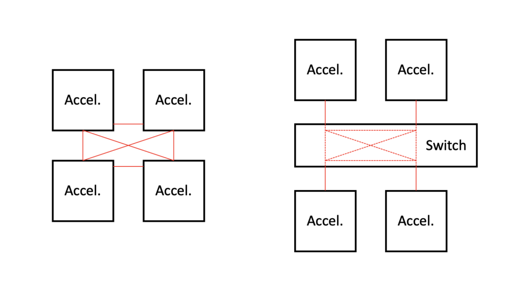
A: Figure 1 shows four AI accelerator chips on a board. The left side shows each chip connected to the others via point-to-point connections, and on the right side, a switch handles the connection of one chip to the others.
Q: What’s the advantage of the switch?
A: Let’s look at Nvidia as an example. For Nvidia, the accelerators are graphical processing units (GPUs), the point-to-point interconnect is called NVLink. The company reports[1] that Nvidia Hopper GPUs can communicate at 900 GB/s with fourth-generation NVLink, but with an eight-GPU configuration, the bandwidth must be shared, and a single point-to-point link is limited to 128 GB/s. Adding Nvidia NVSwitch allows any one of the eight GPUs to talk to any other at the full data rate.
Q: Do other companies have their own approaches?
A: AMD employs its External Global Memory Interconnect (XGMI) for high-speed GPU-to-GPU communications, and the Ultra Accelerator Link Consortium promulgates the UALink standards for facilitating communication between accelerators.
Q: You mentioned chiplets. What exactly is a chiplet?
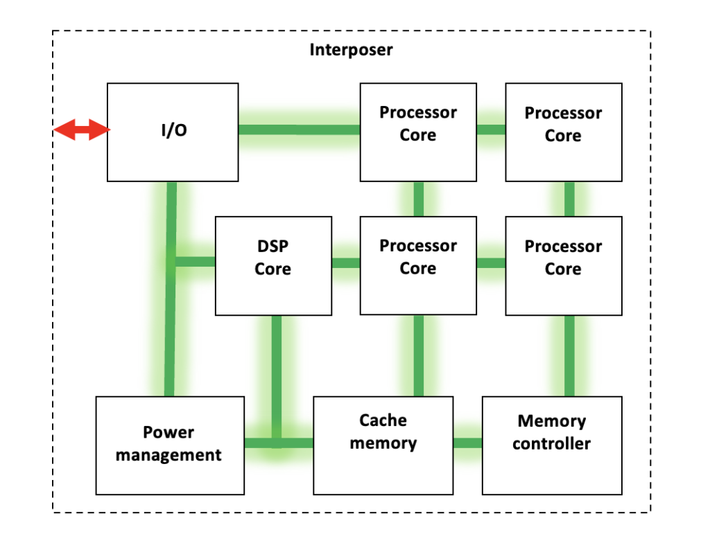
A: A chiplet is a small modular IC that can combine with other chiplets on an interposer to form a more complex device.[2] For example, if you look inside a CPU or system-on-chip (SoC), you might see something like Figure 2, with different interconnected chiplets handling functions such as processing, memory management, and I/O.
Q: Are there standard approaches to chiplet interconnect?
A: Yes. AMD’s approach is called Infinity Fabric[3], on which XGMI is based. In addition, UALink Chiplet Specification 1.0, introduced in April, addresses the integration of UALink technology into chiplet-based SoCs[4].
So that’s a summary of the high-speed interconnect you’re likely to find in a data center.
Q: In part 1, you mentioned USB4….
A: Right. USB4 is an edge-device connector, and it is not commonly found in data centers. It does, however, find use in smart factories, where it can connect to peripherals such as cameras and other sensors, motion controllers, and removable storage. It’s also interesting because it employs three-level pulse-amplitude modulation (PAM3). We looked at PAM4 in an earlier article on PCIe, but we haven’t focused on PAM3.
Q: How does PAM3 work?
A: Figure 3 shows the eye diagrams of waveforms spanning two unit intervals (UIs), where a UI is one-half the waveform period. At the top, we see non-return-to-zero signaling, with one bit transmitted per UI, or two bits per period. At the bottom, we see PAM4, with two bits per UI, or four bits per period, representing any binary number from 0000 to 1111. Then in the middle, we see PAM3, where the signal can take on one of three values per UI.
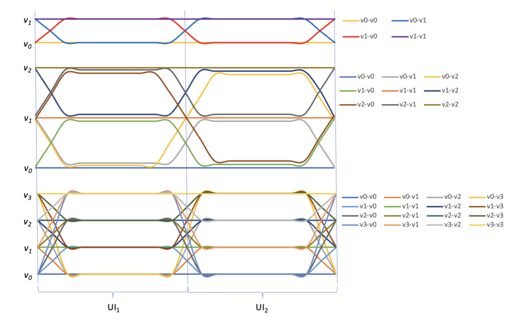
Q: So it looks like PAM3 can transmit 1.5 bits/UI or three bits per period, representing binary 000 to 111, or decimal 0 to 8.
A: Not quite. Note that I’ve offset the waveforms slightly in the PAM3 figure, and if you look closely, you’ll see there are nine possible distinct waveforms — not eight. From Shannon’s information theory, we can calculate the bits/UI as follows:
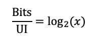
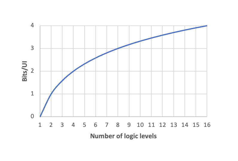
where x is the number of possible logic levels. Figure 4 plots this equation for various logic levels. Note that one UI can carry an integer number of bits for powers of 2. PAM3, on the other hand, carries 1.58 bits/UI.
Q: What instruments do I need to investigate these eye diagrams, and what specifically am I looking for?
A: Jitter is one of the top problems in high-speed communications. We’ll take a look next time.
References
[1] NVIDIA NVLink and NVIDIA NVSwitch Supercharge Large Language Model Inference, Nvidia
[2] What are Chiplets? Synopsys
[3] Engineering the Future of AI: How AMD Interconnects, Infinity Fabric, and Advanced Packaging Drive Scalable Compute, AMD
[4] Ultra Accelerator Link (UALink) Consortium Publishes Four Specifications Defining In-Network Compute, Chiplets, Manageability and 200G Performance, Businesswire
Related EEWorld Online content
What information does an eye diagram depict?
How are NRZ and PAM different in an eye diagram?
What is jitter and what can I do about it (part 1 of 2)?
How accelerator IO interface connectors and cables offer more options
3D IC design for the AI era: an EDA perspective
What you need to know about information theory