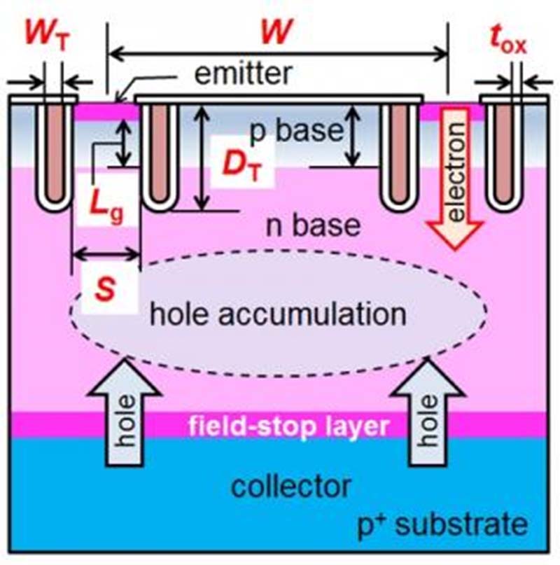
In electronics, lower power consumption leads to operation cost savings, environmental benefits and the convenience advantages from longer running devices. While progress in energy efficiencies has been reported with alternative materials such as SiC and GaN, energy-savings in the standard inexpensive and widely used silicon devices are still keenly sought. K Tsutsui at Tokyo Institute of Technology and colleagues in Japan have now shown that by scaling down size parameters in all three dimensions in their device they can achieve significant energy savings.
Tsutsui and colleagues studied silicon insulated gate bipolar transistors (IGBTs), a fast-operating switch that features in a number of every day appliances. While the efficiency of IGBTs is good, reducing the ON resistance, or the voltage from collector to emitter required for saturation (Vce(sat)), could help increase the energy efficiency of these devices further.

Previous investigations have highlighted that increases in the “injection enhancement (IE) effect”, which give rise to more charge carriers, leads to a reduction in Vce(sat). Although this has been achieved by reducing the mesa width in the device structure, the mesa resistance was thereby increased as well. Reducing the mesa height could help counter the increased resistance but is prone to impeding the (IE) effect. Instead the researchers reduced the mesa width, gate length, and the oxide thickness in the MOSFET to increase the IE effect and so reduce Vce(sat) from 1.70 to 1.26 V. With these alterations the researchers also used a reduced gate voltage, which has advantages for CMOS integration.
They conclude, “It was experimentally confirmed for the first time that significant Vce(sat) reduction can be achieved by scaling the IGBT both in the lateral and vertical dimensions with a decrease in the gate voltage.”

