The automotive industry has made great strides in its efforts to develop and commercialize semi-autonomous and fully autonomous vehicles. With continued innovation in advanced driver assistance systems (ADAS) and accelerating development of 5G network infrastructure, mainstream adoption of driverless cars is approaching ever faster on the horizon. Provided the necessary government safety regulations are in place, we may see fully autonomous vehicles on public roadways by 2021.
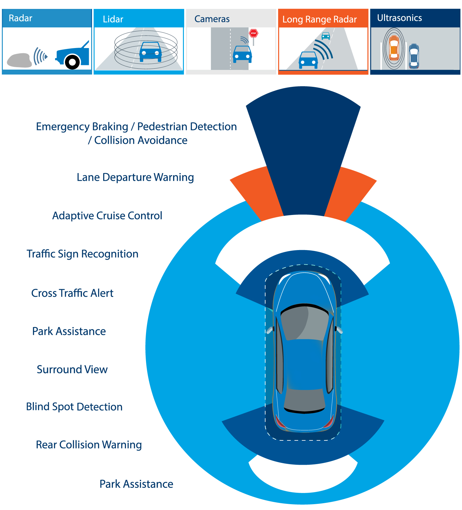
Phase one of this development has centered on the intra-vehicle connectivity needed to centralize and process incoming data from increasing numbers of camera, radar, and LiDAR sensors deployed throughout the vehicle. In subsequent development phases, on-board sensor data will be merged with incoming information from surrounding vehicles and infrastructure, comprising a mesh sensor network that enables “smarter” automatic decision making for improved adaptability to fast-changing driving conditions.
In the meantime, road trials for semi-autonomous vehicles are ongoing, with early prototypes shuttled in and out of R&D labs as the technology is refined. These prototypes are immediately recognizable by the bulky electronic systems mounted on their rooftops and/or squeezed into their trunks, housing the additional sensors, networking, and processing units needed for semi-autonomous operation.
In order for these vehicles to achieve production readiness, these bulky electronic systems will ultimately need to be integrated within the vehicle interior, for reasons that extend beyond aesthetics and available trunk space. In-vehicle integration ensures that the electronics can be adequately climate controlled, protected against harsh weather, and humidity. Historically, the vehicle dashboard has housed the electronics hub, which is likely to continue.
Regardless of how these electronics are integrated, one certainty is the size of PCBs utilized in the connectivity architecture will need to shrink dramatically; from the individual camera, radar, and LiDAR sensors, to the electronic control unit (ECU).
Shifting Gears
To date, automotive system designers have relied on conventional multi-layer PCBs for mechanical and electrical connectivity between components. In recent years, they’ve seen the number of board layers in the ECU grow from six to as many as twelve layers, adding significant design complexity. To meet the system size and integration challenges of sensor-intensive semi-autonomous and autonomous vehicles, system designers will have to eschew multi-layer boards in favor of high-density interconnects (HDIs). Commonly used today in smartphones, smartwatches, and other compact digital devices, HDIs enable more functions per unit area than multi-layer boards by leveraging laser-cut microvia technology, finer lines, and thinner materials.
Having said that, consumer device manufacturers aren’t subject to the stringent safety standards and arduous qualification processes inherent to the automotive industry, where the adoption of HDI technology will therefore be markedly slower. Incumbent automotive PCB suppliers have just begun to build their HDI manufacturing infrastructure, and may need at least two years to qualify their HDIs for use in production vehicles. In the early adoption stages, these suppliers may grapple with yield issues that negatively impact the bottom line.
Precision Handling
Automotive PCB suppliers can accelerate their time to market and time to profitability with HDIs by leveraging advanced laser direct imaging (DI) and automated optical inspection (AOI) systems. These solutions, applied in concert with Industry 4.0 best practices, enable suppliers to increase their manufacturing precision and quality, while improving their production throughput and yield. The benefits of these manufacturing techniques will only compound as more sensors are integrated within next-generation vehicles.
Automotive PCB suppliers can leverage the vast experience of laser DI system suppliers, who can help integrate this capability into their process. DI systems can ensure precision line uniformity, high registration accuracy, and optimal quality even at high production speeds, with the ability to quickly identify and measure panel deformities, instability, and make the necessary adjustments. Advanced automotive applications will require a mix of large HDI boards for connectivity and sensor processing, for which imaging depth of focus is very important to ensure homogenous quality. These applications will also require a mix of small boards at the sensor level, for which high registration capabilities will be needed.
Leveraging advanced AOI systems, automotive PCB suppliers can quickly identify HDI defects, recurring panel defect patterns, and alert production operators in real time to halt the line and/or troubleshoot upstream processes. The sub-micron inspection capabilities enabled by today’s sophisticated AOI systems are increasingly valuable as HDI form factors continue to shrink, and are ideally suited to help meet the stringent quality and reliability requirements of government automotive regulations.
The combination of laser DI and AOI capabilities is particularly beneficial for improving yield. With enhanced visibility into panel and product anomalies, automotive PCB manufacturers can take the necessary steps to refine their production processes, while minimizing wasteful and expensive material scrapping.
With the increased need for safety electronics units in semi- and fully autonomous cars, traceability of components throughout the manufacturing process becomes mandatory. When a faulty card is identified, supply chain traceability enables a manufacturer to confirm the specific process that yielded the failure. Each PCB must therefore have a unique ID that can be traced back to the specific manufacturer, along with the process of manufacturing and handling.
This adheres to Industry 4.0 best practices that are already implemented at leading PCB fabricators, where traceability solutions are integrated within the DI, AOI, and other systems to allow automatic recording of all manufacturing stages, with clear visibility and data sharing for OEMS across the supply chain. The traceability itself is serving as a source for data analyses, enabling faster New Product Introductions (NPIs) as process are refined.
The Road Ahead
There’s no longer a question “if” autonomous cars will achieve mainstream commercial viability, but when. Taking into account the myriad passenger safety and transportation efficiency benefits, autonomous vehicles hold the promise to fundamentally transform land-based travel, shipping, and commerce for future generations.
In the near term, automotive system designers will focus increased attention on optimizing system form factors and integration, ensuring that additional sensors and ECUs required for semi-autonomous and autonomous vehicles can be readily incorporated within a sleek end design. Automotive PCB suppliers will play a crucial role in this innovation. The precision manufacturing and inspection capabilities enabled with advanced laser DI and AOI systems will ultimately allow these suppliers to mirror the progress achieved in the consumer device domain with HDI technology, while ramping up process efficiencies, improving yield, and driving greater profitability. The combination of new production tools with comprehensive data management and traceability will enable a fast ramp up to a new era of innovation in the automotive industry.
