Optoelectronic sensors typically limit their response to one or more specific ranges of the optical spectrum. Ambient light sensors will suppress responses to wavelengths outside the visible spectrum, while IR sensors suppress responses to visible and shorter wavelengths. Interference filters have high value characteristics, such as high band pass transmissions, low stop band transmissions, and sharp transitions, and are an excellent tool to limit the response to specific wavelength ranges.
Interference filters are constructed with thin layers of dielectric material, as shown in figure 1:
|
Material |
Refractive Index (λ = 550 nm) |
|---|---|
|
SiO2 |
1.4599 |
|
Al2O3 |
1.7704 |
|
HfO2 |
2.1174 |
|
Ta2O5 |
2.1411 |
|
Nb2O5 |
2.3603 |
|
TiO2 |
2.6479 |
By selecting the appropriate refractive index and the thickness of the layers, specific wavelengths are allowed to be transmitted through the filter, creating the pass band region, or reflected, creating the stop band region. Since the stop band low transmission is a result of reflection, very little optical power is absorbed.
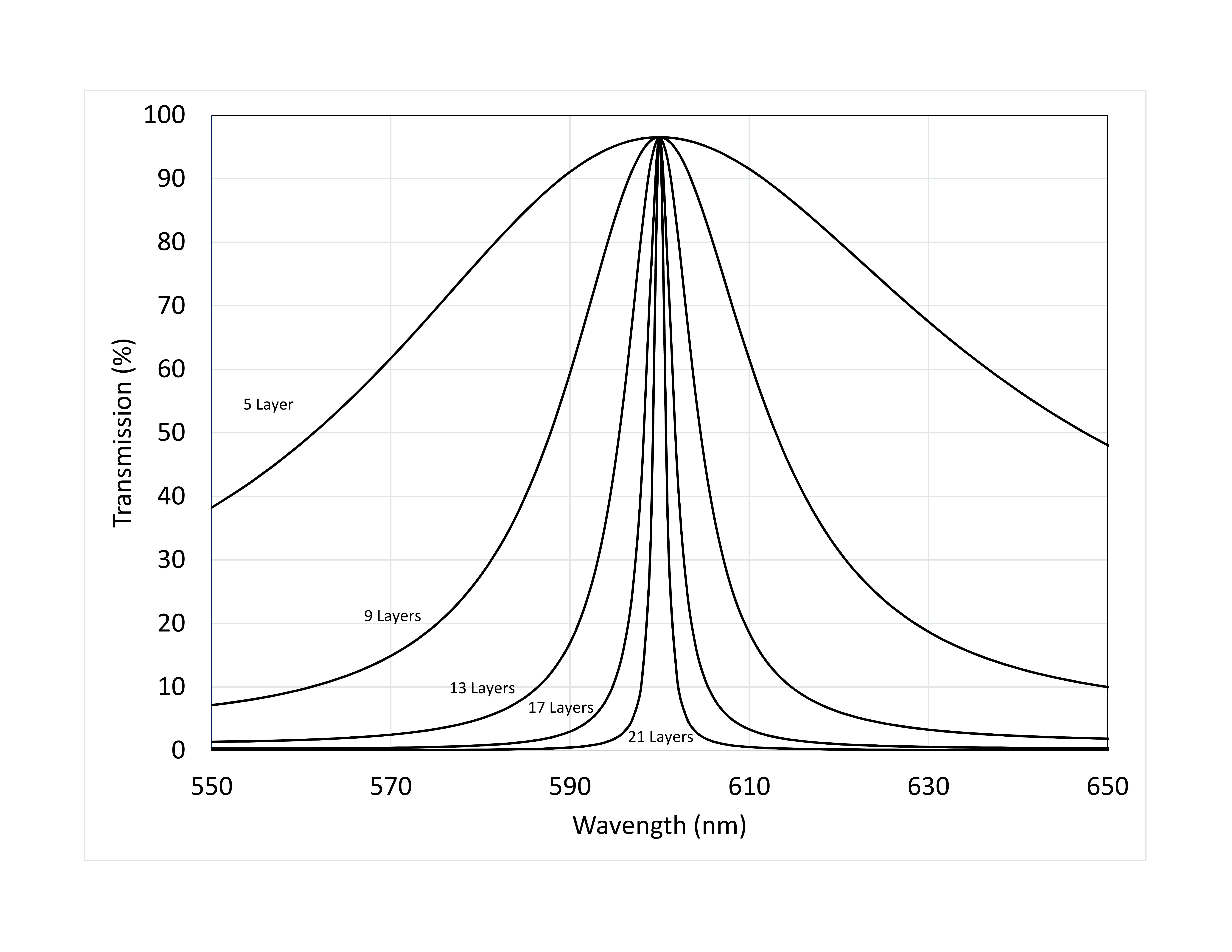
Multiple layers are stacked to create sharper transitions from the pass band to the stop band regions (figure 2).
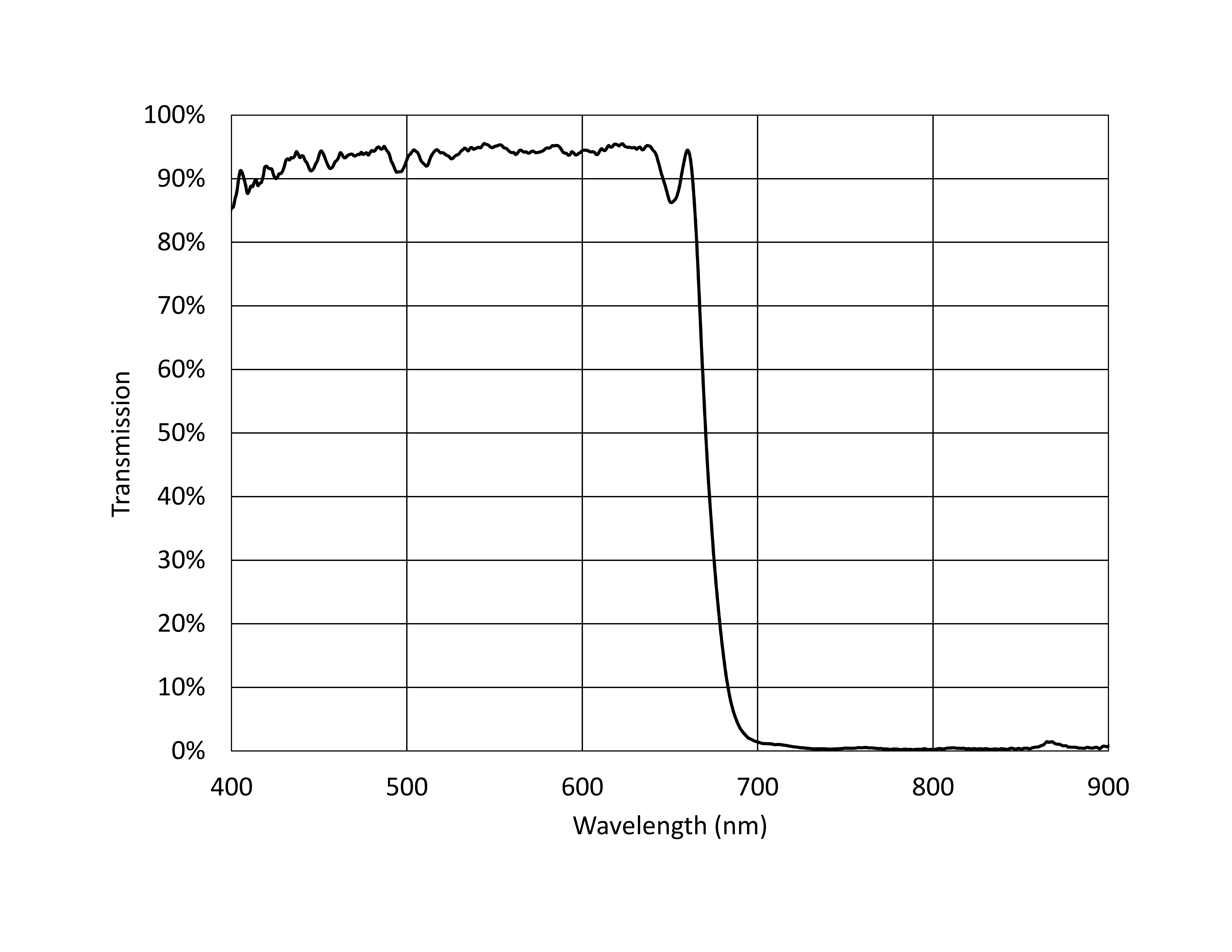
The long pass, short pass, and notch filters typically use 100 more layers to form sharp transitions. Even with the high number of layers, the pass band wavelengths maintain a high transmission exceeding 90 percent, while the stop band wavelength transmission is less than 1 percent. The filter transition can be as low as 10 nm. Figure 3 is an example of an interference filter with the purpose of passing visible wavelengths and blocking infrared wavelengths.
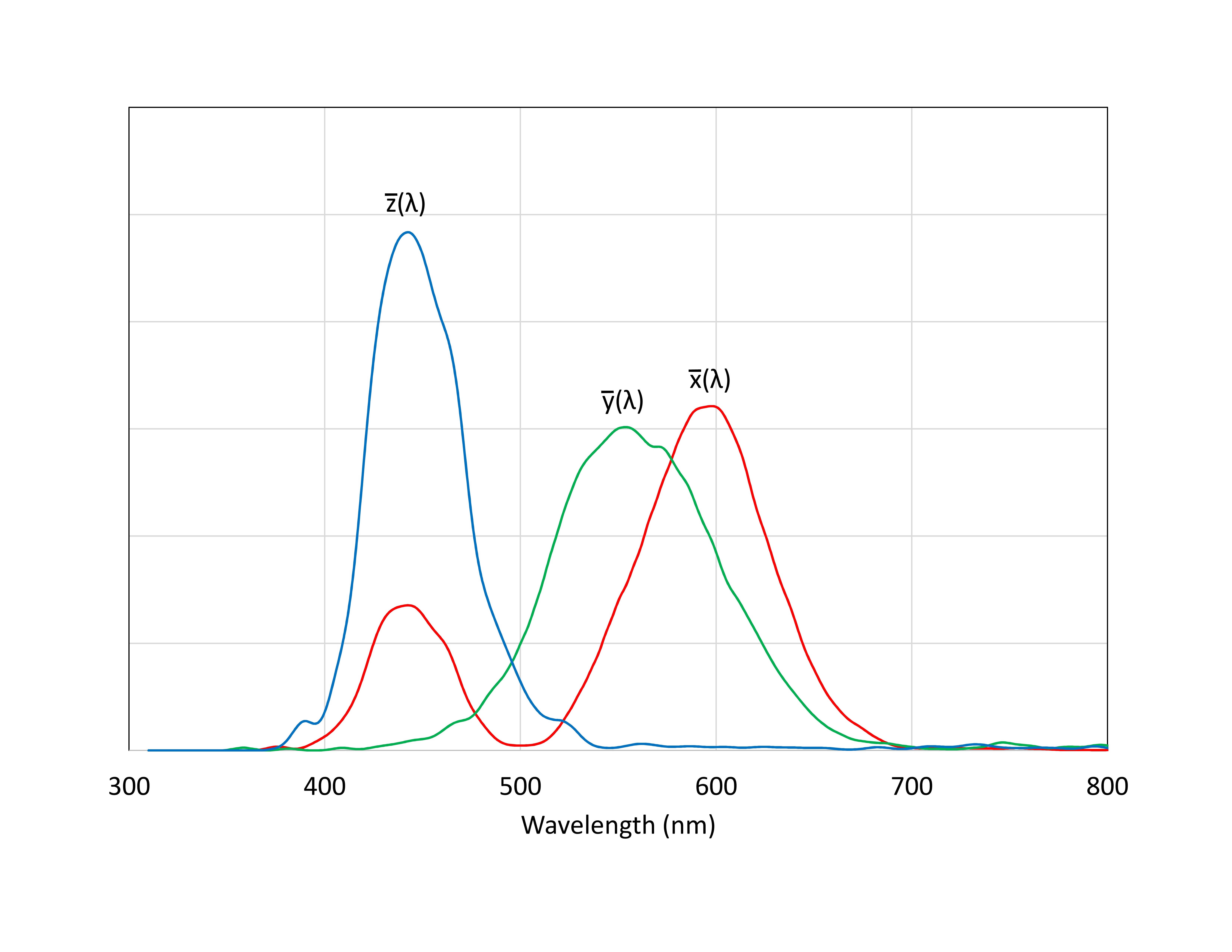
By reducing the layer count and introducing additional refractive indexes, interference filters can also have weighted responses with slower transitions. Sensor designs can benefit greatly by adding a weighted response that allows the sensor to duplicate specific optical functions and provide more information on the object or source being monitored. A good example of the optical function replicated by a filter is the Tristimulus function used for color analysis (figure 4).
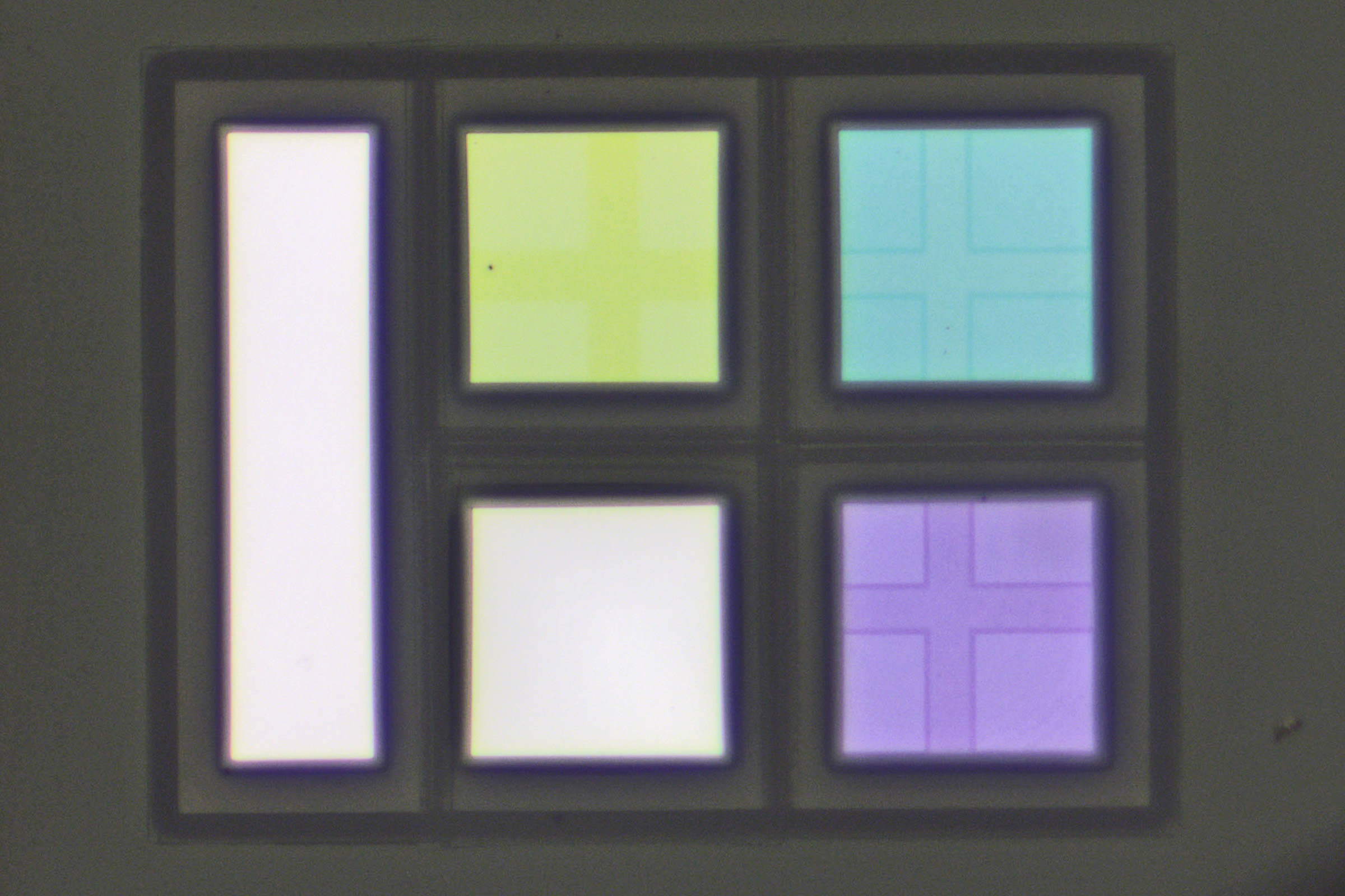
Without being able to duplicate the optical function using filters, a more complicated and costly spectral scan will be needed to acquire the same information. Multiple filter layer depositions and etching processes on semiconductors allow the designer to specify the unique weighted optical functions for each independent channel on the semiconductor die, creating a sensor in a single package with multiple functions, saving cost and space and improving system reliability. Figure 5 shows an example of a multi-channel sensor with narrow band filters on two IR channels (near-white reflection) and Tristimulus function filters on the remaining channels (colored reflection).
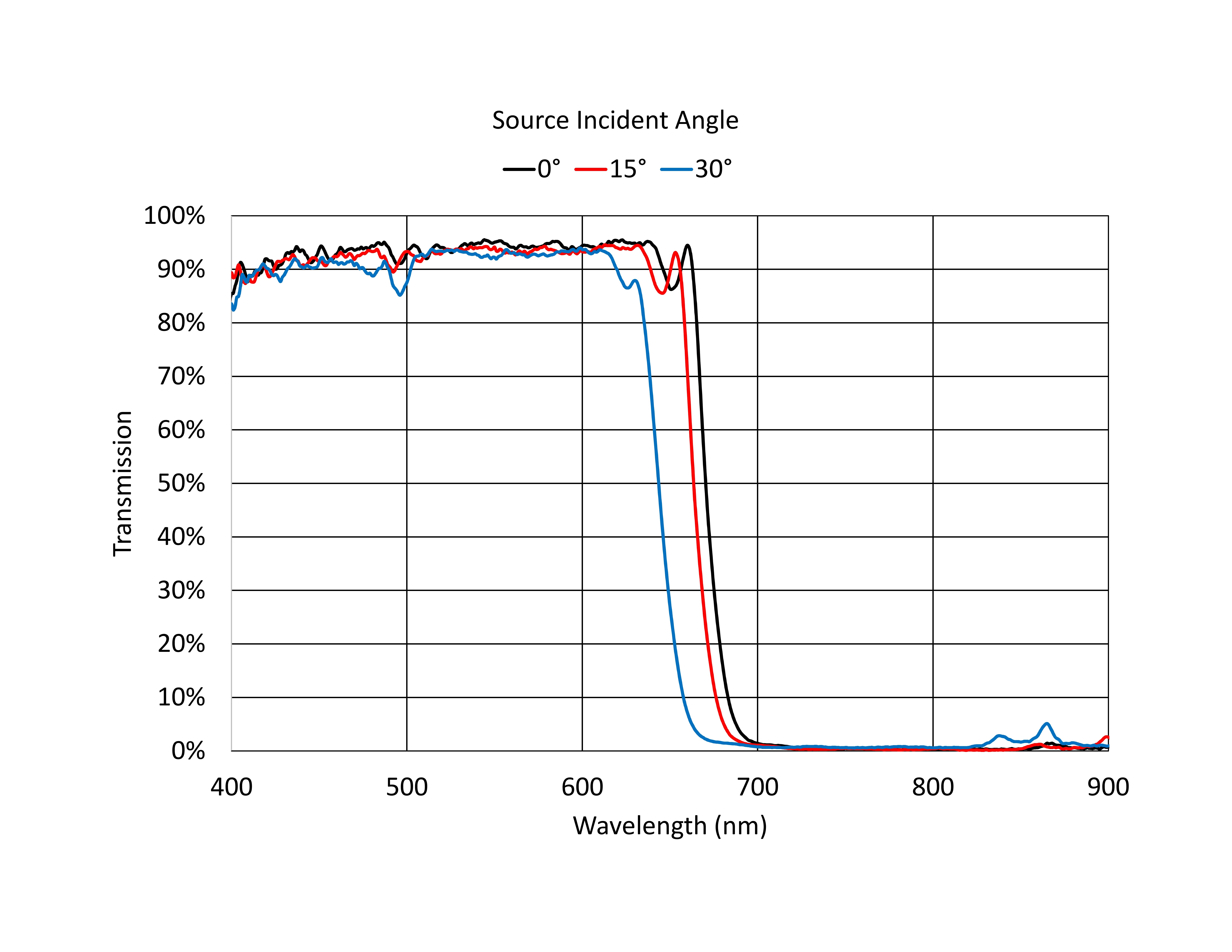
An interference filter characteristic that needs to be considered for designs is the sensor acceptance angle. As the illuminance source incident angle increases, the interference filter characteristics will change. The stop band transmission will increase, and the transition wavelength will shift as the source incident angle increases (figure 6).
Limiting the sensor field of view will naturally minimize this effect. If the field view needs to be larger, a diffuser can be incorporated into the optical stack. The diffuser redirects the optical energy in random directions independently of the source angle. The system acceptance angle can be restricted by the geometric relationship of the diffuser aperture opening, the sensor active area, and the distance between the sensor and diffuser (figure 7).
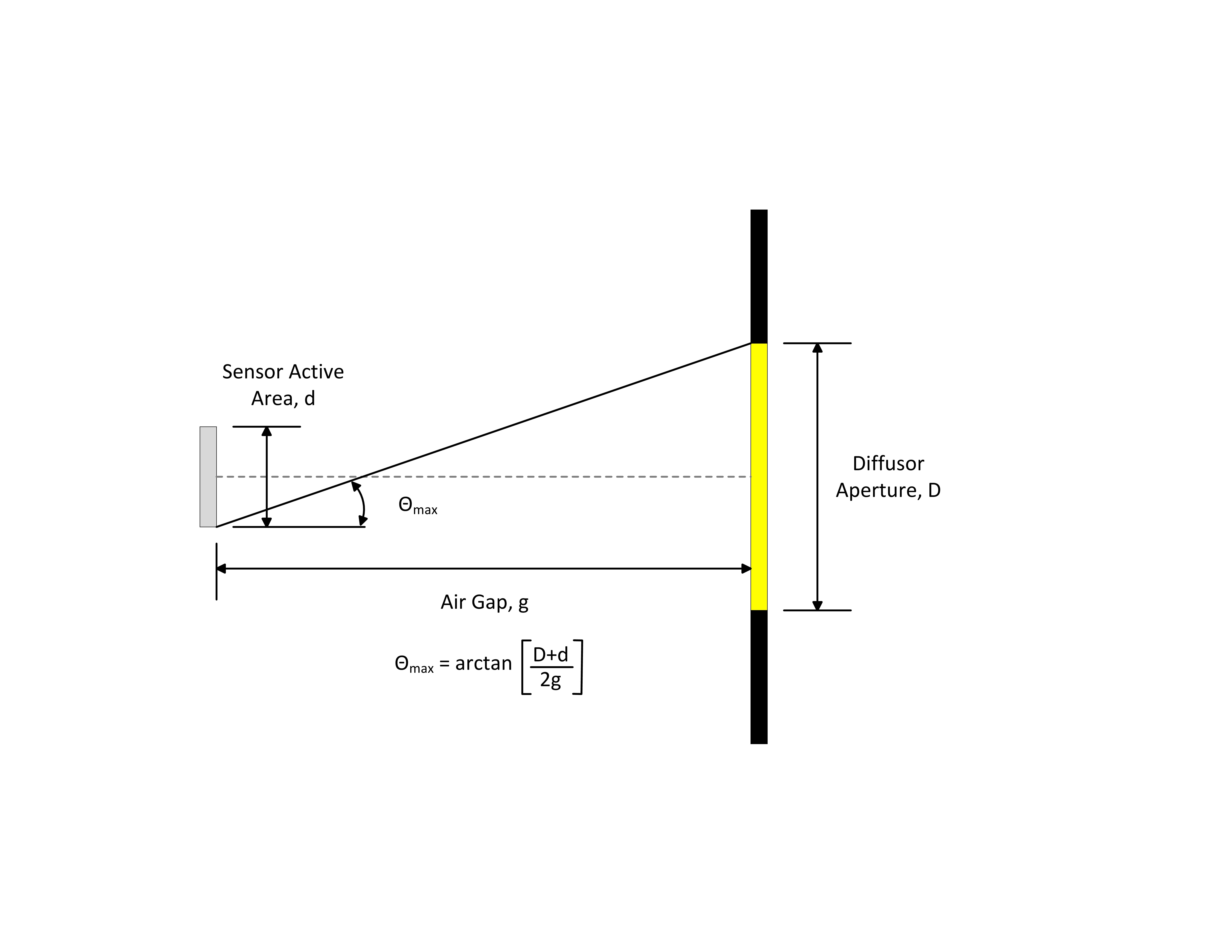
The diffuser will not eliminate the incident angle effect on the sensor, however, it will make the system response more stable with respect to the source incident angle. This allows for a simpler system level design to accommodate the skewed spectral response related to larger source incident angles.
Organic filters are alternate options to interference filters and do not have the same sensitivity to source incident angles as interference filters do. However, organic filters do not have the same capability as interference filters to match optical functions and efficiency. Further, organic filters have a lower operating and storage temperature than interference filters.
Low-temperature sputtering manufacturing process and lift off technology enables the interference filter to have low sensitivity to changes in temperature and exposure to high humidity. Advanced deposition processing techniques ensure the filter is of high quality and operates well in harsh environments. Best in-class manufacturers will incorporate in-process control monitors for layer thickness and material uniformity to ensure low tolerances are maintained. A plasma sputtering process combined with optical rapid feedback produce a closely controlled film stoichiometry structure.
Software is available to model the interference filter design and optimize the shape to match the desired transmission characteristics. Additional considerations for the sensor design optimization is compensating for the silicon spectral response and the effects of the optical stack. Incorporating the manufacturer process tolerances into the filter analysis is crucial for a robust design.
The optical filter transmission shape and sensor channel gain are key to fulfilling the optical function design requirements that enable simple, reliable, and cost effective solutions. It is advantageous to work with a semiconductor manufacturer to ensure successful delivery of the optical function-based sensor design and product.

