Today, RF and microwave systems such as radar, benefit from lowering size, weight, power, and cost (SWaP-C) of systems and RF equipment. Cost refers to reducing both operating (OPEX) and capital expenditure costs (CAPEX). OPEX reductions are achievable by focusing on higher performance to reduce energy consumption (with higher efficiency), or extending a system’s service lifetime (with higher reliability). CAPEX reductions can be achieved by lowering component and development costs, along with reducing development time for environmentally robust solutions.
Gallium nitride (GaN) has intrinsic advantages in speed-power product, widely recognized in the RF/microwave market today. Consequently, common circuit applications like high power amplifiers (HPAs), low noise amplifiers (LNAs) with high signal survivability, and dynamic range, as well as high power switches are using GaN. In radar applications specifically, the performance of GaN HPAs and robustness of GaN LNAs allow greater flexibility in T/R functional diagrams, superior performance, and reduce total cost. High-performance T/R implementations are more viable without size, weight, and cost compromises of circulators, isolators, and limiters.
The integration of GaN technology with die-level environmental robustness enables the powerful combination of superior RF performance and dramatic reductions in packaging cost and size, and that capability is available today. Some examples of gallium arsenide (GaAs) Monolithic Microwave Integrated Circuit (MMIC) technology achieved this level of environmental robustness more than a decade ago. GaN has been a greater challenge, since its higher operating voltages accelerate mechanisms dominating environmental stress degradation. These requirements are often assessed by HAST, THB, or other environmental stress tests.
Testing Standards and Previous Work on GaAs Technology
Temperature, humidity, bias testing (THB), highly accelerated temperature, and humidity stress testing (HAST) are often used interchangeably to qualify semiconductor products for operation in uncontrolled environments (non-hermetic packaging). A typical international test and compliance standard for HAST testing is JEDEC JESD22-A110. The THB test is 1000 hours at 85°C, 85 percent relative humidity (RH), while the HAST test lasts 96 hours at 130°C, 85 percent RH. Both tests are designed to provide accelerated time testing of how the product or technology will perform in moist environments, providing lifetime performance estimates. The two tests are considered equivalent for silicon products using aluminum metallization. Therefore, the HAST test is often used for convenience and cost-effectiveness, as it can be run in a timeframe of days, rather than weeks.
For compound semiconductor products using GaAs and GaN technologies, there can be a discrepancy between the two, depending on the corrosion mechanism’s activation energy due to temperature, humidity, and bias conditions. Sometimes, vendors will choose to only apply temperature and humidity stress (no bias) to products. This test standard is typically referred to as unbiased HAST (uHAST). While this is a valid test standard, omission of voltage bias doesn’t adequately simulate product operation in the real world. Additionally, voltage bias may significantly contribute to corrosion mechanisms within a tested technology that may limit operational lifetime. So, it’s important to understand the effect of bias combined with temperature in a moist environment.
Previous work to develop and validate a GaAs 0.15 μm gate length acceleration model, pHEMT technology was completed in 2015. This highlights the importance of understanding the underlying semiconductor failure theory and completing a technology testing regime to assure the product level environmental test is relevant for moisture compliance qualification. Applying the testing standard blindly could lead to significant differences in equivalency between the THB and HAST tests. Moisture-induced failure accelerating factors need to be similar in value to those established for silicon-based technologies, to assume 1000 hours of THB testing is equivalent to 96 hours of HAST testing.
Initial moisture tests on GaN technology obtained equivalent results from both THB and HAST testing. These results were in line with previous work completed on GaAs technology.
GaN Moisture Compliant Products
GaN transistor products with peak output power capability ranging from 10 W to 220 W, were used to assess die-level HAST ruggedness for 28 V and 48 V operation. Two examples of GaN transistor products are shown in Figure 1. Achieving die-level HAST compliance allows using packaging solutions for products to provide low cost and additional enhanced features like low thermal resistance. Low thermal resistance provides system operators a range of benefits such as higher DC to RF efficiency, extended life, or higher ambient temperature operation.
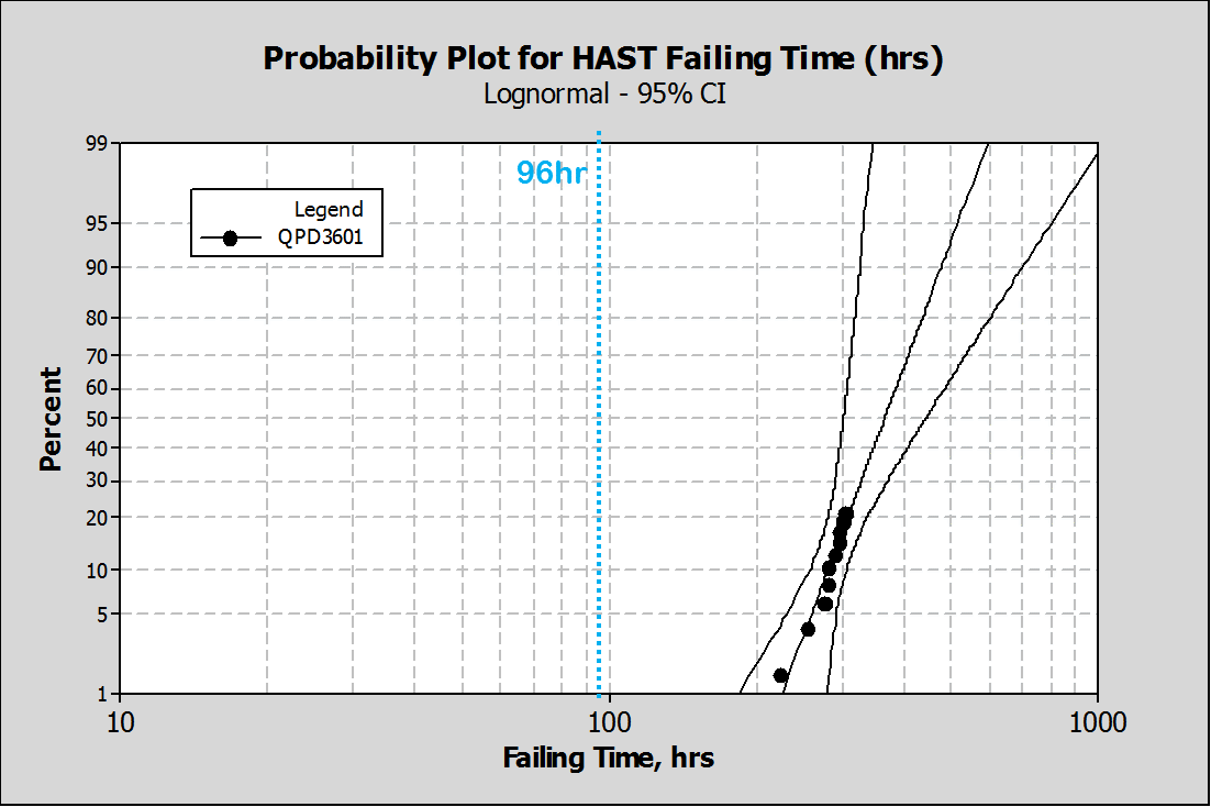
GaN die were assembled in unsealed air cavity packages for moisture testing. Unsealed packages were used to focus moisture stress on the GaN die, rather than the die and package combination. Devices were pre-screened after assembly using a pinch-off test. During HAST testing, bias voltages were applied to the device, but no DC current was flowing. Bias conditions were monitored for the stress test duration, during which individual failure times were recorded as they occurred. The failure criterion was a catastrophic short. HAST tests were run for an extended period of time, beyond the test standard goal of 96 hours to obtain several failure points. Results were then fit with a log-normal distribution. Figure 2 shows an example of time-to-fail HAST test results for a GaN product with 220 W peak RF output power. As one can see, the devices tested have considerable margin beyond the 96-hour criteria. Data shows the product passes two times the JEDEC standard criteria, with first failure after applying more than 200 hours of continuous stress.
While THB and HAST testing are used interchangeably in the RF component qualification industry, the standard cannot be applied blindly and needs the semiconductor context being used. For compound semiconductors like GaAs and GaN, validating the acceleration factors is essential for product qualification testing to be relevant. Examples of high voltage operation GaN technology with moisture ruggedness at the die level are available to enable low-cost, high-performance RF component solutions.
