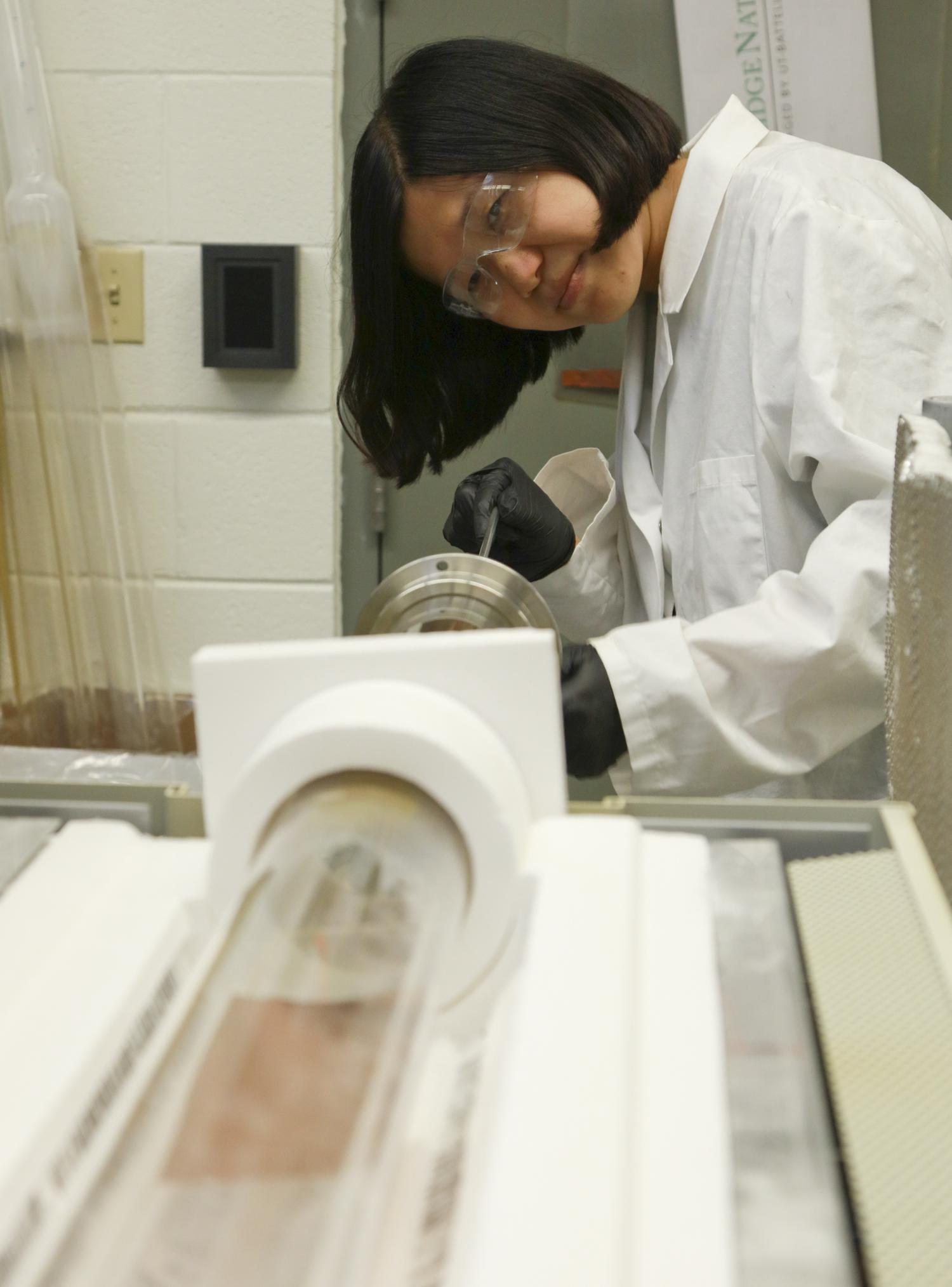
A new era of electronics and even quantum devices could be ushered in with the fabrication of a virtually perfect single layer of “white graphene,” according to researchers at the Department of Energy’s Oak Ridge National Laboratory.
The material, technically known as hexagonal boron nitride, features better transparency than its sister, graphene, is chemically inert, or non-reactive, and atomically smooth. It also features high mechanical strength and thermal conductivity. Unlike graphene, however, it is an insulator instead of a conductor of electricity, making it useful as a substrate and the foundation for the electronics in cell phones, laptops, tablets and many other devices.
“Imagine batteries, capacitors, solar cells, video screens and fuel cells as thin as a piece of paper,” said ORNL’s Yijing Stehle, postdoctoral associate and lead author of a paper published in Chemistry of Materials. She and colleagues are also working on a graphene hexagonal boron 2-D capacitor and fuel cell prototype that are not only “super thin” but also transparent.
With their recipe for white graphene, ORNL researchers hope to unleash the full potential of graphene, which has not delivered performance consistent with its theoretical value. With white graphene as a substrate, researchers believe they can help solve the problem while further reducing the thickness and increasing the flexibility of electronic devices.
While graphene, which is stronger and stiffer than carbon fiber, is a promising material for data transfer devices, graphene on a white graphene substrate features several thousand times higher electron mobility than graphene on other substrates. That feature could enable data transfers that are much faster than what is available today. “Imagine your message being sent thousands of times faster,” Stehle said.
Stehle noted that this work is especially significant because it takes the material beyond theory. A recent theoretical study led by Rice University, for instance, proposed the use of white graphene to cool electronics. Stehle and colleagues have made high-quality layers of hexagonal boron nitride they believe can be cost-effectively scaled up to large production volumes.
“Various hexagonal boron nitride single crystal morphology – triangle to hexagon – formulations have been mentioned in theoretical studies, but for the first time we have demonstrated and explained the process,” Stehle said.
That process consists of standard atmospheric pressure chemical vapor deposition with a similar furnace, temperature and time, but there’s a twist. The difference is what Stehle describes as “a more gentle, controllable way to release the reactant into the furnace and figuring out how to take advantage of inner furnace conditions. These two factors are almost always neglected.”
Stehle continued: “I just thought carefully beforehand and was curious. For example, I remind myself that there are many conditions in this experiment that can be adjusted and could make a difference. Whenever I see non-perfect results, I do not count them as another failure but, instead, another condition adjustment to be made. This ‘failure’ may become valuable.”
Co-authors of the paper.are Harry Meyer, Raymond Unocic, Michelle Kidder, Georgios Polizos, Panos Datskos, Roderick Jackson and Ivan Vlassiouk of ORNL and Sergei Smirnov of New Mexico State University. Funding was provided by the Laboratory Directed Research and Development program. A portion of the research was conducted at the Center for Nanophase Materials Science, a DOE Office of Science User Facility at ORNL.

