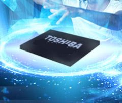
Toshiba Memory America, Inc. says it has started sampling the industry’s first Universal Flash Storage (UFS) Ver. 3.0 embedded flash memory devices. The new lineup utilizes the company’s cutting-edge 96-layer BiCS FLASH 3D flash memory and is available in three capacities: 128 gigabytes, 256 GB and 512 GB. With high-speed read/write performance and low power consumption, the new devices target applications such as mobile devices, smartphones, tablets, and augmented/virtual reality systems.
Sample shipments of the 128 GB device will start 1-22-2019 with the rest of the line-up to  gradually follow after March. Specification of the samples may differ from that of commercial products.
Universal Flash Storage (UFS) is a product category for a class of embedded memory products built to the JEDEC UFS standard specification. Due to its serial interface, UFS supports full duplexing, which enables both concurrent reading and writing between the host processor and UFS device.
Product density is identified based on the density of memory chip(s) within the Product, not the amount of memory capacity available for data storage by the end user. Consumer-usable capacity will be less due to overhead data areas, formatting, bad blocks, and other constraints, and may also vary based on the host device and application. The definition of 1 GB = 230 bytes = 1,073,741,824 bytes.
Consumers continue to demand increasingly higher performance and an improved user experience from their devices, and the UFS standard is constantly being refined in order to support this evolution. With the introduction of UFS 3.0, JEDEC, the global leader in the development of standards for the microelectronics industry, has enhanced previous versions of the UFS standard to help product designers enable significant improvements in mobile devices and related applications.
“As the first company to introduce UFS samples back in early 2013, Toshiba Memory Corp.’s introduction of UFS Ver. 3.0 embedded flash memory devices is further proof that we continue to be at the forefront of storage for next-gen mobile devices,” noted Scott Beekman, director of managed flash memory products for Toshiba Memory America, Inc.
The new devices integrate 96-layer BiCS FLASH 3D flash memory and a controller in a JEDEC-standard 11.5×13-mm package. The controller performs error correction, wear leveling, logical-to-physical address translation, and bad-block management for simplified system development.
All three devices comply with JEDEC UFS Ver. 3.0, including HS-GEAR4, which has a theoretical interface speed of up to 11.6 Gigabits/sec/lane (x2 lanes = 23.2 Gbps) while also supporting features that suppress increases in power consumption. Sequential read and write performance of the 512GB device are improved by approximately 70 percent and 80 percent, respectively, over previous generation devices[5].
For more information, please visit business.toshiba-memory.com.
Toshiba Memory America Inc., 2610 Orchard Pkwy, San Jose, CA 95134, (408) 526-2700, www.toshiba.com/TMA


Leave a Reply
You must be logged in to post a comment.