Among the presentations at this year’s IEDM: A silicon vacuum transistor that operates at over 38 kV.
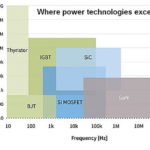
Examine a hospital x-ray machine or a high-power RF transmitter and you’ll find a beefy vacuum tube. Vacuum devices still rein for applications requiring extremely high voltages (>30 kV) such as for x-ray generation or high-power radar (> 10 kW). But a special kind of “vacuum” transistor maybe able to begin taking over these applications.
So say researchers from M.I.T. and Mass. General Hospital in Boston. In a paper to be presented at the upcoming IEEE International Electron Devices Meeting (“Demonstration of a ~40 kV Si Vacuum Transistor as a Practical High Frequency and Power Device,” W. Chern et al, MIT/Harvard/Massachusetts General Hospital), the group describes the first steps toward a practical high-voltage vacuum transistor. The device uses a cold-cathode field emission electron source and experimentally demonstrates a current density and voltages which enable its use as both a next generation x-ray source and a high-power and frequency device.

One big problem with existing high-power vacuum tubes is their use of a heated filament (>2,000°C) as a source of electrons. This thermionic electron source is slow to turn on and off and gets hot, so ancillary electronics must be kept at a distance. The vacuum transistor has neither drawback, says the group. Getting rid of the thermionic source lets other parts of the transistor sit close to the electron source enabling high electric fields needed to make a compact device that can outperform solid-state devices on all metrics.
The vacuum transistor consists of three components: an electron source comprised of silicon field emitter arrays (Si FEAs), a vacuum package and a metal anode. Silicon FEAs are field-emission devices consisting of a sharp silicon tip with a diameter < 10 nm, designed to concentrate an electric field, in series with a ballast resistor or a high-aspect-ratio silicon nanowire. The Si FEAs can be mass-produced via chip fabrication techniques. Si FEAs and the anode are connected through multi-channel vacuum feedthroughs and wire bonded on a package. These nanowires are embedded in a dielectric matrix and controlled by a conductive (polysilicon) gate.
The group cautions that while vacuum transistors have extremely promising intrinsic figure of merits, the technology is still at an early-stage. For one thing, vacuum packaging (~10-8 torr) must be developed that can withstand the high voltages involved. Vacuum packaging able to meet the electric field requirements of the transistors has yet to be demonstrated. And the capacitance involved in the transistor parts currently sits at ~50 aF/tip, limiting realizable frequencies to 1-10 GHz assuming the device is not transit-time limited. The current cross-over between capacitance and transit time limitations occurs ~100 kV. They also say that further optimization of the electron source could improve the device enabling higher frequencies and lower voltages to become interesting.
The 66th annual edition of the IEEE International Electron Devices Meeting (IEDM), the world’s premier forum for the presentation of applied research in transistors and related devices, will take place virtually this year. The conference will now run from Saturday through Friday, December 12-18, 2020, and will offer a mix of live-streamed events and on-demand pre-recorded presentations, with a schedule of live Q&A sessions. The expanded schedule is intended to give global attendees enough time to review the more than 220 papers in the IEDM technical program, plus the tutorials and short courses, and to participate in the live-streamed events, such as the plenary presentations, panel discussion and career session.
This year’s theme is “Innovative Devices for a Better Future,” which reflects the fact that, at a time of great global uncertainty, electronics technology is being used much more broadly than ever before to address the world’s most pressing challenges.
“This year’s format may be different, but what hasn’t changed at all is that IEDM will once again offer an outstanding technical program that showcases important breakthroughs in key semiconductor and related technologies, which are essential for the progress of modern society,” said Dina Triyoso, IEDM 2020 Publicity Chair and Technologist at TEL Technology Center, America, LLC. “I’m very proud of the fact that, despite the laboratory restrictions and all of the other challenges imposed on us by the pandemic, our community has persevered and driven the state-of-the-art of electronics technology forward yet again.”
“Although a virtual experience doesn’t give us the ability to see our colleagues in person, it does provide unique opportunities which we have tried to maximize,” said Meng-Fan (Marvin) Chang, IEDM 2020 Publicity Vice Chair, IEEE Fellow, Distinguished Professor of Electrical Engineering at National Tsing Hua University and Director of Corporate Research at TSMC. “For example, if IEDM were a physical event this year, nine technical sessions would run in parallel. An attendee likely would find it difficult to attend all talks of interest. But with recorded presentations available on-demand a week ahead of time, that roadblock is eliminated.”