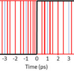
Electronic noise results in spurious signals (spurs) or distortion in amplitude, frequency or both. Jitter refers to unwanted variation in frequency, particularly in digital pulses and typically in the clock signal. Timing disruptions negatively impact system performance, particularly in ADCs, where sampling occurs, and in DACs. We’ll discuss causes of jitter, its detection and measurement using time and frequency domain instrumentation, and mitigation procedures.
Time-varying signals including jitter are quantified in terms of RMS or peak-to-peak in terms of displacement and spectral density, which describes the distribution of power into frequency components. Obtaining this information requires the Fourier Transform and Fourier Analysis, accessed by applying the signal to the input of a spectrum analyzer or of an oscilloscope in RF or Math>FFT mode. Spectral density as a function of power is by convention expressed as watts per hertz (W/Hz).
 Clock jitter is quantified by three principle metrics:
Absolute jitter is a measure of the absolute difference between a clock edge as specified and its observed position.
Period (cycle) jitter is a measure of the difference between and observed clock period and the ideal or average clock period.
Cycle-to-cycle jitter is a measure of observed durations between adjacent clock periods.
Types of jitter are:
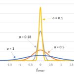
Random (Gaussian) jitter is caused by electronic timing noise. It is unpredictable but in the statistical long run, conforms to a normal distribution curve. It is always present, the result of thermal noise that exists in any conductor, component or circuit.
Deterministic jitter, so-named because it is reproducible and may be predicted. It has a peak-to-peak value that is bounded. The distribution is known, conforming to non-normal distribution.
Total jitter is the sum of random and deterministic jitter. Random jitter adds broadband noise to the signal of interest. Periodic jitter introduces erroneous spectral elements.
At higher frequencies, jitter disrupts signal conversion to a great extent.
Jitter can be further characterized as correlated or uncorrelated. Correlated jitter is in close correspondence to a noise source. It is usually periodic. Correlated jitter that is aperiodic is more difficult to diagnose. Multiple noise sources may make correlated jitter appear to be uncorrelated.
Uncorrelated (random) jitter is a consequence of the intrinsic thermal noise that is an additive product of all conductors and components in every system. There is no outside noise source.
Clock jitter can be measured as follows:
Maximum-time interval error jitter and phase-noise measurements often include period jitter and cycle-to-cycle jitter. These measurements require an ideal clock for reference. Maximum, typical and minimum differences are recorded.
Peak cycle-to-cycle jitter is the maximum difference between adjacent, consecutive clock signals.
Peak-to-peak period jitter is the difference between longest and shortest clock periods within a specified time interval.
Jitter is measured in the time domain. The same phenomenon, measured in the frequency domain, is generally known as phase noise. The oscilloscope invariably has a higher noise floor than the spectrum analyzer. In both instruments, the noise floor places a limit on the lowest amplitude signal that can be displayed. The oscilloscope measures peak-to-peak and cycle-to cycle jitter. The spectrum analyzer cannot directly measure these parameters. Instead, it measures phase noise. Deterministic spurs are readily accessed and displayed. In the time domain, the oscilloscope can display lower-frequency clock signals as well as signals with data-dependent jitter.

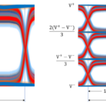
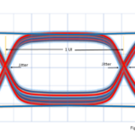
Eye diagram: A digital signal is periodically sampled and applied to an oscilloscope vertical input. The data rate triggers the horizontal sweep.
One approach to locating the source of jitter is to inject jitter into critical electronic components. Measurements are then performed on serial bus media, typically displaying them in the form of eye diagrams. Close examination of the eye diagram suggests various measurements:
Eye crossing, amplitude and percentage
Eye height, level and signal-to-noise ratio
Vertical eye opening
Quality factor
Deterministic jitter
Eye crossing time, delay, fall time, rise time, width and horizontal opening
Peak-to-peak, random, RMS, CRC and total jitter
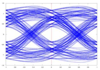
Synchronized superimposed cycles with infinite persistence illustrate small variation. The degree to which the eye closes corresponds to noise in the signal.
Eye width measures timing synchronization and timing effects. Eye closure measures additive noise and inter-symbol interference. Height and peak-to-peak eye opening measures additive signal noise. Eye overshoot and undershoot measure peak distortion due to signal path interruptions.
In telecommunications, jitter is a serious issue. As in all electronics, it is the deviation from the true periodicity of a presumably periodic signal, generally in reference to the clock.
In networks, jitter is a different although related phenomenon. It occurs within longer timeframes in contrast to jitter at the intra-waveform level. Network jitter is responsible for latency in video streaming, voice-over-Internet dead spots and the Live TV discontinuities that we see every day. Simply put, it is due to differences in packet arrival time.
Suppose packets are sent at a reasonable rate–for example, one frame every 10 msec–but due to Internet bottlenecks, they are received at one frame every 11 msec. Those delays will cause interruptions – you see the spinning circle for a few seconds rather than the programming as broadcast, or in VOIP your phone conversation is interrupted. (VOIP is more prone to network jitter than is streaming video because the packets are smaller.)
A partial remedy is the jitter buffer, which is a piece of hardware in which voice or other packets can remain for limited intervals, then proceed to the processor at a uniform rate, eliminating packet loss. Where effective, this strategy counters network congestion, timing drift and significant delays due to rerouting. Poor performance results when the jitter buffer is incorrectly sized. If it is too small, an excessive number of packets may be discarded. If it is too large, packets undergo additional delay. This implementation can partially control, but may not totally eliminate, network jitter. Jitter buffers are currently being offered by email spammers, with verbiage indicating that the revolutionary device is to be plugged into the homeowner’s modem.
Besides jitter buffers, successful mitigation techniques include anti-jitter circuits, filtering, decomposition and dejitterizing. It is feasible to build anti-jitter circuits, which work best when the jitter-prone signal of interest is a regular pulse signal. Anti-jitter circuits retime the output so that it becomes a high-quality pulse. Common varieties are the phase-locked loop and the delay-locked loop.
A phase-locked loop in its simplest form consists of a controller whose phase at the output relates to the signal phase at the input. A widely-used type consists of a variable-frequency oscillator and a phase detector comprising a feedback loop. The oscillator is continuously adjusted to synchronize input and output phases. A delay-locked loop is similar, but the internal voltage-controlled oscillator is replaced by a delay line. A delay-locked loop generates an error signal based on the phase of its last output, comparing it to that of the input clock. An error signal is subsequently integrated and used to control the delay element(s).
Delay lines have been used in a great many applications. They may be mechanical, often acoustic, or purely electronic. Basic to the electronic delay line is the fact that any RC or RLC circuit has an inherent time constant. Electronic delay lines exploit the property of any capacitor and resistor connected in series to discharge the voltage stored in the capacitor. The time constant, known as τ, is expressed by:
τ = RC
Where R = resistance in ohms; C = capacitance in farads. This constant is equal to the time required to charge a capacitor through a resistor to 63.2% of the applied voltage, or to discharge it to 36.8% of the full charge. These percentages are derived from the value of e-1.
The delay of a conductor, conductive component or circuit derives from the RC time constant in conjunction with distance. The delay of these elements in an LC circuit derives from the LC time constant in conjunction with the speed of light. Either RC or LC circuits (actually RLC since all conductors contain a finite amount of resistance) form the basis for electronic delay lines and are useful in combating network jitter.