3D printing is the fabrication of a three-dimensional object under computer control, with one or more materials being added layer by layer. 3D printing, or additive manufacturing, is used across various electronics applications, including circuit boards, energy storage devices, actuators, and sensors. It can be implemented using a variety of technologies, including selective laser sintering (SLS), stereolithography (SLA), fused filament fabrication (FFF), direct ink writing (DIW), and inkjet printing.
4D printing (also called 4D bioprinting, active origami, or shape-morphing systems) uses the same techniques like 3D printing, but 4D printing adds the dimension of time and produces an object that can change its shape or other parameters over time. 4D printing produces a programmable material that responds to environmental inputs such as humidity, light, or temperature and transforms into another structure. This FAQ will consider the application of 3D and 4D printing in circuit boards, energy storage, sensors, actuators, sensors, and solar panels. The next FAQ will review specific applications of 3D printing in 5G systems.
3D printed circuit boards
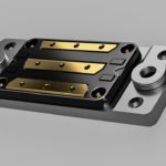
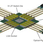
3D printing is being used to make printed circuit boards (PCBs) for a growing variety of applications. These PCBs can be used for prototyping, short production runs, for their unique properties, or a combination of reasons. For example, impedances in 3D circuit boards can be precisely controlled, and 3D circuit boards can be designed with multiple layers of high density interconnects and embedded components that enable the board’s surface to accommodate a high component density. Multiple power and ground planes can be used in the interior layers, enhancing isolation, EMC compliance, and power and signal integrity.
Mixed-signal PCBs can especially benefit from the use of 3D printing. 3D PCBs can now withstand the soldering process needed to place components on both sides of a PCB using a recently developed dielectric polymer ink and conductive ink. Those new inks have been used to fabricate a 10-layer PCB with high-performance electronic devices soldered to both sides. This capability can be instrumental in high-performance military sensor systems.

Multi-layer 3D printed circuit boards can also include embedded and 3D printed capacitors, resistors, and magnetic devices such as transformers and inductors in the various layers. Plus, a variety of integrated circuits and other semiconductor devices can be embedded.
3D-printed supercapacitors
Energy storage devices such as batteries and supercapacitors can limit the performance of exploration systems operating in extremely cold environments such as Earth’s polar regions and Mars. On Mars, for example, temperatures can dive to -62 C (-81 F) at night, and heaters are required to keep batteries from freezing. Those heaters consume energy that could otherwise be used for exploration activities.
Scientists recently 3D printed a porous carbon aerogel using cellulose nanocrystal-based ink and used the resulting structure to fabricate a supercapacitor capable of operating at -70 C (-94 F). The electrodes are printed into a matrix structure which is then freeze-dried, and a surface treatment is applied. The result is a porous structure with holes measuring 500 microns across. In addition, there are smaller pores in the beams of the printed matrix structure. These smaller nanometer-scale pores allow ion diffusion and charge transfer through the electrode.
The printed structure is called a 3D multiscale porous aerogel (3D-MCA). It has a very large surface area that enables it to achieve high capacitance at low temperatures. In addition, it retains that capacitance at high charge/discharge rates. Compared with 3D-MCAs produced with other fabrication methods, the 3D-printed aerogel retains its capacitance 6.5 times better.
3D-printed sensors
3D printing allows the fabrication of low-cost sensors based on resistive and capacitive technologies. The sensors can have a unique shape and size that can be printed directly into the robot’s fingers. In the case of resistive sensors, as the fingers flex while grasping an object, each conductor deforms slightly, and its resistance changes, providing a simple way to monitor and control a robotic hand for grasping small objects.
3D printed capacitive touch sensors have been printed directly on the fingertips of a robot hand. In addition, interface electronics was developed to produce a digital output based on changes in the capacitance, enabling touch feedback control. 3D printed electrodes were fabricated using a copper-based conductive filament and a two-part printed flexible rubber dielectric. The capacitive touch pressure sensor has two soft capacitive sensors that resemble the fingertip of a human thumb. The device is 30mm long, 20mm wide, and 8.3mm thick, and the overlapping areas of the parallel capacitive sensors are 163.24 mm-square with a dielectric thickness of 1 mm.
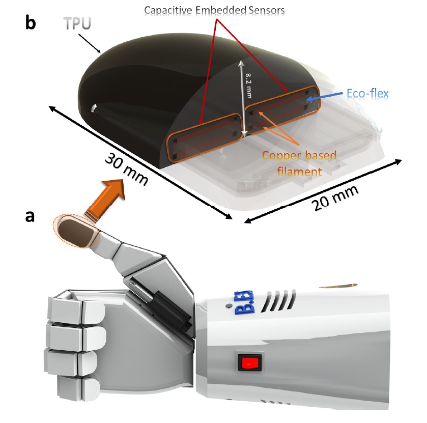
The touch sensor has a capacitance of about 4 pF. The sensor was tested under static and dynamic conditions. Static testing included linear loading and unloading from 0 to 25 N. Dynamic testing included loading and unloading the sensor from 0 to 15 N for 200 cycles at 1 cycle per second. Both tests indicate that the sensors have the high repeatability that is necessary for practical applications. In addition to being used in a robot hand, this type of capacitive sensing is expected to find use in instrumented objects in various applications. Printed resistive and capacitive sensors are sometimes classified as 4D-printed objects.
4D-printed sensors
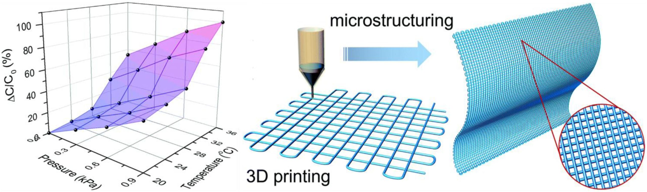
Soft tactile sensors (STSs) consist of several parts: a flexible substrate, flexible electrodes, and sensing elements. STSs are fabricated using 3D printing to precisely control the spatial relationships between the various materials to endow the final structure with mechanical and/or electric transducing capabilities. Because the function of the structure changes over time in response to external stimuli, it’s called 4D printing.

In addition to the resistive and capacitive sensor technologies discussed above, STSs can be fabricated using other phenomena such as
- Piezoelectric STSs produce a voltage as a result of applied mechanical stress or deformation. They can have high sensitivity and fast response time and are used to detect dynamic pressure, such as sound and sliding vibration. In addition, the energy harvesting capabilities of piezoelectric materials enable the design of low-power or self-powered tactile sensors.
- Magnetoelectric STSs – are an emerging technology for tactile sensors that uses a magnetic field to convert mechanical pressure into electrical signals. Based on electromagnetic induction, these STSs are self-powered and do not require an external power source.
3D- and 4D-printed actuators
Miniaturized actuators made using electroactive polymer (EAP) technology are difficult to produce with conventional photolithographic processes. 3D printing processes are being developed specifically to produce EAP macrobiotic actuators for use in miniaturized robots. 3D printing is expected to simplify the fabrication of EAP actuators, making them cost-effective across a larger range of applications.
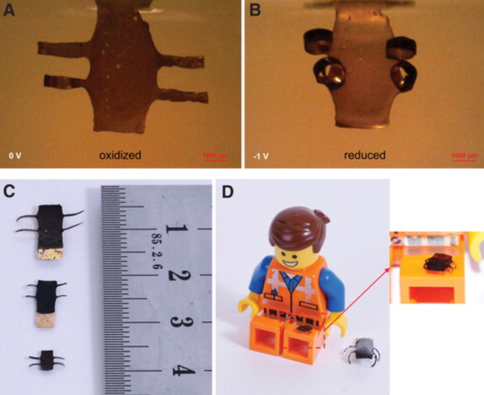
One development effort 3D printed three microrobots, measuring 6 × 4.5 mm2, 7 × 9.5 mm2, and 14 × 12 mm2, each with four micro actuator limbs. The limbs can be driven with an activation voltage of -1.0 V, simplifying their integration into systems. These microrobots can potentially be used to grasp and release objects or as micro walkers. The micro actuators have to be combined with ionogels or other solid state ion sources in a trilayer actuator to enable air operation.
In another example of electroactive actuators, a 3D printed hybrid structure with thermoplastic/ conductor bilayers was fabricated that can be actuated by differential heating caused by externally controllable currents flowing through their conducting faces. The resulting flexible structures propel the robot forward using step-wise applied voltages. Using higher currents to generate more elevated temperatures can result in irreversible deformations, a form of 4D printed structure that can also enlarge the linear response range of the actuators. With the proper drive circuit, it is possible to alternatively drive both layers of a bilayer structure into very large deformations in a process called ratcheting. Heating protocols where multiple areas are actuated in sequence open the door to various very large and easily controllable deformations of 3D printed hybrid materials.
Printed photovoltaics
3D photovoltaic (PV) panels are made using organic semiconductor polymer inks. The ink can be printed over plastic surfaces, or even steel, which means those printed solar panels could be embedded into buildings. Currently, PET (polyethylene terephthalate) is often used as the substrate. The 200-microns thick printed PV panels are about 4-times the thickness of a human hair.
Because the active layers are thin, over 99% of the panel material is the PET substrate. That can be an advantage since PET is relatively inexpensive and it is recyclable. Conventional crystalline PV panels are not easily recycled, with many ending up in landfills. With the printed PV panels, the PET substrates can be recycled and used to make new PVs.
Unfortunately, the efficiency of these printable solar panels is still an order of magnitude less than crystalline PV panels. On the other hand, printed PV panels can be inexpensive, with an anticipated production cost of less than $10 per square meter. Compared with crystalline silicon, the raw materials used to produce the printed solar panels are inexpensive.
 Printed solar panels are low-cost, flexible, and recyclable but currently too inefficient to be practical. (Image: University of Newcastle)
Summary
Circuit boards, energy storage devices, actuators, and sensors are just some of the devices made using 3D printing. 4D printing uses the same techniques as 3D printing, but 4D printing uses various “active” materials to enable an object to change its shape or other parameters over time. 4D printing is expected to be especially useful for producing sensors and actuators, especially for robot platforms and wireless internet of things (IoT) devices. For more insights into how 3D printing is used in electronics, check out the next two FAQs in this series: “3D printing for 5G systems” and “Advanced power electronics packaging.”
References
3D Printed Robotic Hand with Embedded Touch Sensors, University of Glasgow
3D Printing Microactuators for Soft Microrobots, Soft Robotics
3D Printed Actuators: Reversibility, Relaxation and Ratcheting, Cornell University
4D Printing: A technology coming from the future, Sculpteo
New multi-layer PCB boosts electronics rapid prototyping, Hensoldt
Printing Porous Carbon Aerogels for Low Temperature Supercapacitors, Nano Letters
Public Debut for Printed Solar, University of Newcastle
Recent Advances of 4D Printing Technologies Toward Soft Tactile Sensors, Frontiers in Materials