• Skip to primary navigation
  • Skip to main content
  • Skip to primary sidebar
  • Skip to footer

Electrical Engineering News and Products

Electronics Engineering Resources, Articles, Forums, Tear Down Videos and Technical Electronics How-To's

  • Products / Components
    • Analog ICs
    • Battery Power
    • Connectors
    • Microcontrollers
    • Power Electronics
    • Sensors
    • Test and Measurement
    • Wire / Cable
  • Applications
    • 5G
    • Automotive/Transportation
    • EV Engineering
    • Industrial
    • IoT
    • Medical
    • Telecommunications
    • Wearables
    • Wireless
  • Learn
    • eBooks / Handbooks
    • EE Training Days
    • Tutorials
    • Learning Center
    • Tech Toolboxes
    • Webinars & Digital Events
  • Resources
    • White Papers
    • Design Guide Library
    • Digital Issues
    • Engineering Diversity & Inclusion
    • LEAP Awards
    • Podcasts
    • DesignFast
  • Videos
    • EE Videos and Interviews
    • Teardown Videos
  • EE Forums
    • EDABoard.com
    • Electro-Tech-Online.com
  • Bill’s Blogs
  • Advertise
  • Subscribe

Improving transimpedance amplifiers with a bootstrap

June 10, 2021 By Chris Francis Leave a Comment

Analog bootstrap circuits are traditionally ones where output is fed back to the input, usually to increase input impedance. This can be to minimize either the resistive or reactive (usually capacitive) components of the input impedance or both. The term is now also used with MOSFET drivers where a capacitor is charged and used to pump up a voltage for gate drive. This article is concerned with reducing the effect of the gate-drain capacitance of a JFET in a transimpedance amplifier. The technique can also be used for bipolar circuits or HEMT or GaAsFET transistors and can be extended to also reduce the effects of photodiode capacitance.

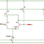
A typical idealized JFET input transimpedance amplifier could be represented like this:

 transimpedance amplifiers

I1, R3 and C1 represent the photodiode with some dark current (leakage) and 0.5pF of capacitance. The JFET is shown as a source follower with an ideal gain stage E2 following it. V2 is used to level shift for biasing. This arrangement would give around 96MHz of bandwidth. One reason for using a source follower for the first stage rather than a common source amplifier is that you will need a unity gain stage for bootstrapping but also because the source follower will have a wider bandwidth than a common source amplifier. The disadvantage is that the noise performance of a common source based circuit is likely to be better than one based on a source follower.

Adding a bootstrap as shown below will roughly double the bandwidth to 183MHz.

transimpedance amplifier

The bootstrapping can be further extended to include the photodiode. This can be particularly helpful where the photodiode has a large capacitance.

Analog

For example, with 5pF of photodiode capacitance, bootstrapping the JFET has very little effect because the input capacitance is dominated by the photodiode not the JFET. However, bootstrapping the photodiode will increase the bandwidth from 24MHz to 81MHz. Then bootstrapping the JFET will further increase that to 130MHz because the effective photodiode capacitance has been reduced and the JFET gate-drain capacitance is significant again. Bootstrapping the JFET on its own will only increase the bandwidth from 24MHz to 27MHz. Real-life circuits will not be quite as good depending on how they are implemented.

The unity gain buffer required for the bootstrap might be implemented with an emitter follower in which case its gain will be less than unity. However, if an opamp were used then the performance would be better. Similarly, the gain stage will not have infinite bandwidth. Overall though, the technique is very useful in trying to design high transimpedance, high bandwidth transimpedance amplifiers for photodiodes, including avalanche photodiodes. The techniques can be used with custom IC-based implementations as well as discrete circuits, and for circuits with discrete devices mixed with opamps.

As with any circuit of this nature, the circuit noise should also be analyzed as well, and transient simulations carried out to check there are no undesirable effects under certain circumstances/conditions. This would include the effect of a significant DC current in the photodiode if that was a possible operating condition for the circuit.

You Might Also Like

Filed Under: Analog IC Tips, Analog ICs, FAQ, Featured Tagged With: FAQ

Reader Interactions

Leave a Reply Cancel reply

You must be logged in to post a comment.

This site uses Akismet to reduce spam. Learn how your comment data is processed.

Primary Sidebar

EE Engineering Training Days

engineering

Featured Contributions

Five challenges for developing next-generation ADAS and autonomous vehicles

Robust design for Variable Frequency Drives and starters

Meeting demand for hidden wearables via Schottky rectifiers

GaN reliability milestones break through the silicon ceiling

From extreme to mainstream: how industrial connectors are evolving to meet today’s harsh demands

More Featured Contributions

EE Tech Toolbox

“ee
Tech Toolbox: Internet of Things
Explore practical strategies for minimizing attack surfaces, managing memory efficiently, and securing firmware. Download now to ensure your IoT implementations remain secure, efficient, and future-ready.

EE Learning Center

EE Learning Center
“ee
EXPAND YOUR KNOWLEDGE AND STAY CONNECTED
Get the latest info on technologies, tools and strategies for EE professionals.
“bills

R&D World Podcasts

R&D 100 Episode 10
See More >

Sponsored Content

Advanced Embedded Systems Debug with Jitter and Real-Time Eye Analysis

Connectors Enabling the Evolution of AR/VR/MR Devices

Award-Winning Thermal Management for 5G Designs

Making Rugged and Reliable Connections

Omron’s systematic approach to a better PCB connector

Looking for an Excellent Resource on RF & Microwave Power Measurements? Read This eBook

More Sponsored Content >>

RSS Current EDABoard.com discussions

  • Reducing "shoot-through" in offline Full Bridge SMPS?
  • What is the purpose of using a VCVS?
  • Checking line impedance
  • Why do I hear whistling sounds in my vents?
  • Mains inverter with switching node going out on the mains cable!?

RSS Current Electro-Tech-Online.com Discussions

  • Why can't I breadboard this oscillator?
  • Failure of polypropylene motor-run capacitors
  • a point I can't understand about the sinc expression
  • Quick advice on remote car starter?
  • Wideband matching an electrically short bowtie antenna; 50 ohm, 434 MHz
Search Millions of Parts from Thousands of Suppliers.

Search Now!
design fast globle

Footer

EE World Online

EE WORLD ONLINE NETWORK

  • 5G Technology World
  • Analog IC Tips
  • Battery Power Tips
  • Connector Tips
  • DesignFast
  • EDABoard Forums
  • Electro-Tech-Online Forums
  • Engineer's Garage
  • EV Engineering
  • Microcontroller Tips
  • Power Electronic Tips
  • Sensor Tips
  • Test and Measurement Tips

EE WORLD ONLINE

  • Subscribe to our newsletter
  • Teardown Videos
  • Advertise with us
  • Contact us
  • About Us

Copyright © 2025 · WTWH Media LLC and its licensors. All rights reserved.
The material on this site may not be reproduced, distributed, transmitted, cached or otherwise used, except with the prior written permission of WTWH Media.

Privacy Policy